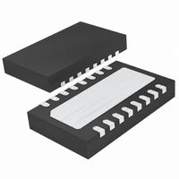
LTC4267CDHC#PBF Linear Technology, LTC4267CDHC#PBF Datasheet - Page 14

LTC4267CDHC#PBF
Manufacturer Part Number
LTC4267CDHC#PBF
Description
IC POE 802.3AF INTERFACE 16-DFN
Manufacturer
Linear Technology
Datasheet
1.LTC4267IGNPBF.pdf
(32 pages)
Specifications of LTC4267CDHC#PBF
Controller Type
Power over Ethernet Controller (POE)
Interface
IEEE 802.3af
Current - Supply
3mA
Operating Temperature
0°C ~ 70°C
Mounting Type
Surface Mount
Package / Case
16-DFN
Linear Misc Type
Negative Voltage
Package Type
DFN EP
Operating Supply Voltage (max)
-57V
Operating Temperature (min)
0C
Operating Temperature (max)
70C
Operating Temperature Classification
Commercial
Product Depth (mm)
3mm
Product Length (mm)
5mm
Mounting
Surface Mount
Pin Count
16
Lead Free Status / RoHS Status
Lead free / RoHS Compliant
Voltage - Supply
-
Lead Free Status / Rohs Status
Compliant
Available stocks
Company
Part Number
Manufacturer
Quantity
Price
LTC4267
APPLICATIO S I FOR ATIO
14
regulator is not disabled during the current-limited turn-on
sequence, the PD circuitry will rob current intended for
charging up the load capacitor and create a slow rising
input, possibly causing the LTC4267 to go into thermal
shutdown.
The ⎯ P ⎯ W ⎯ R ⎯ G ⎯ D pin connects to an internal open drain, 100V
transistor capable of sinking 1mA. Low impedance to
V
ance during signature and classifi cation probing and in
the event of a thermal overload. During turn-off, ⎯ P ⎯ W ⎯ R ⎯ G ⎯ D
is deactivated when the input voltage drops below 30V.
In addition, ⎯ P ⎯ W ⎯ R ⎯ G ⎯ D may go active briefl y at turn-on for
fast rising input waveforms. ⎯ P ⎯ W ⎯ R ⎯ G ⎯ D is referenced to the
V
tential. Connect the ⎯ P ⎯ W ⎯ R ⎯ G ⎯ D pin to the switching regulator
circuitry as shown in Figure 7.
the LTC4267 will attempt to quickly charge capacitor C1
using an internal secondary current limit circuit. In this
scenario, the PSE current limit should provide the overall
limit for the circuit. For slower rising inputs, the 375mA
current limit in the LTC4267 will set the charge rate of the
capacitor C1. In either case, the ⎯ P ⎯ W ⎯ R ⎯ G ⎯ D signal may go
inactive briefl y while the capacitor is charged up to the
new line voltage. In the design of a PD, it is necessary
to determine if a step in the input voltage will cause the
⎯ P ⎯ W ⎯ R ⎯ G ⎯ D signal to go inactive and how to respond to this
event. In some designs, it may be desirable to fi lter the
⎯ P ⎯ W ⎯ R ⎯ G ⎯ D signal so that intermittent power bad conditions
are ignored. Figure 7 demonstrates a method to insert a
lowpass fi lter on the power good interface.
For PD designs that use a large load capacitor and also
consume a lot of power, it is important to delay activation
of the switching regulator with the ⎯ P ⎯ W ⎯ R ⎯ G ⎯ D signal. If the
PSE
PORTN
PORTN
TO
V
LTC4267
PORTN
pin and when active, will be near the V
indicates power is good. ⎯ P ⎯ W ⎯ R ⎯ G ⎯ D is high imped-
Figure 6. LTC4267 Power Good
U
THERMAL SHUTDOWN
UVLO
U
–
+
+
–
1.125V
300k
W
PWRGD
I
TH
PGND
/RUN
300k
P
4267 F06
OUT
R9
100k
MIN
U
5µF
PORTN
C1
+
PGND
po-
PD Interface Thermal Protection
The LTC4267 PD Interface includes thermal overload
protection in order to provide full device functionality
in a miniature package while maintaining safe operat-
ing temperatures. Several factors create the possibility
of signifi cant power dissipation within the LTC4267. At
turn-on, before the load capacitor has charged up, the
instantaneous power dissipated by the LTC4267 can be
as much as 10W. As the load capacitor charges up, the
power dissipation in the LTC4267 will decrease until it
reaches a steady-state value dependent on the DC load
current. The size of the load capacitor determines how
fast the power dissipation in the LTC4267 will subside. At
room temperature, the LTC4267 can typically handle load
capacitors as large as 800µF without going into thermal
shutdown. With large load capacitors, the LTC4267 die
temperature will increase by as much as 50°C during a
single turn-on sequence. If for some reason power were
removed from the part and then quickly reapplied so that
the LTC4267 had to charge up the load capacitor again, the
temperature rise would be excessive if safety precautions
were not implemented.
The LTC4267 PD interface protects itself from thermal
damage by monitoring the die temperature. If the die
PSE
TO
PSE
TO
–48V
–48V
ALTERNATE ACTIVE-HIGH ENABLE FOR P
SEE APPLICATIONS INFORMATION SECTION
I
V
TH
PORTN
Figure 7. Power Good Interface Examples
/RUN
P
V
LTC4267
VCC
PORTN
LTC4267
PWRGD
ACTIVE-HIGH ENABLE FOR RUN PIN WITH INTERNAL PULL-UP
V
PORTP
PGND
P
PWRGD
V
OUT
PORTP
PGND
P
OUT
+
+
C1
5µF
100V
R9
100k
C1
5µF
100V
PGND
R18
10k
R9
100k
PGND
VCC
R18
10k
PIN
D6
MMBD4148
0.047µF
D6
MMBD4148
0.047µF
C15
C15
FMMT2222
FMMT2222
Q1
Q1
C17
R
START
C
PVCC
REGULATOR
I
GND
SWITCHING
TH
AUXILIARY
LTC3803
OPTIONAL
/RUN
4267fc
4267 F07


