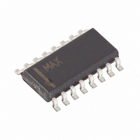
MAX5941ACSE+T Maxim Integrated Products, MAX5941ACSE+T Datasheet - Page 3

MAX5941ACSE+T
Manufacturer Part Number
MAX5941ACSE+T
Description
IC IEEE 802.3AF-COMP POE 16-SOIC
Manufacturer
Maxim Integrated Products
Datasheet
1.MAX5941ACSE.pdf
(24 pages)
Specifications of MAX5941ACSE+T
Controller Type
Power over Ethernet Controller (POE)
Interface
IEEE 802.3af
Voltage - Supply
48V
Current - Supply
1mA
Operating Temperature
0°C ~ 70°C
Mounting Type
Surface Mount
Package / Case
16-SOIC (3.9mm Width)
Lead Free Status / RoHS Status
Lead free / RoHS Compliant
ELECTRICAL CHARACTERISTICS (continued)
(V
unless otherwise noted. Typical values are at T
ELECTRICAL CHARACTERISTICS (PWM Controller)
(All voltages referenced to V-. V
SS_SHDN, NDRV = open circuit, OPTO = V-, T
UVLO External Reference Voltage
Hysteresis
UVLO Bias Current
UVLO Input Ground Sense
Threshold
UVLO Input Ground Sense Glitch
Rejection
Power Turn-Off Voltage,
Undervoltage Lockout Deglitch
Time
Isolation Switch N-Channel
MOSFET On-Resistance
Isolation Switch N-Channel
MOSFET Off-Threshold Voltage
GATE Pulldown Switch Resistance
GATE Charging Current
GATE High Voltage
PGOOD, PGOOD Assertion V
Threshold
PGOOD, PGOOD Assertion V
Threshold
PGOOD Output Low Voltage
PGOOD Output Low Voltage
PGOOD Leakage Current
PGOOD Leakage Current
SUPPLY CURRENT
V+ Supply Current
V+ Supply Current After Startup
V
IN
DD
= (GND - V
Supply Current
IEEE 802.3af-Compliant Power-Over-Ethernet
PARAMETER
PARAMETER
Interface/PWM Controller for Power Devices
EE
) = 48V, GATE = PGOOD = PGOOD = OPEN, V- tied to OUT, V+ tied to GND, UVLO = V
_______________________________________________________________________________________
OUT
GATE
DD
= 13V, a 10µF capacitor connects V
SYMBOL
V
I
I
VDD(NS)
I
SYMBOL
V
TH,G,UVLO
t
V+(NS)
VDD(S)
I
V
OFF_DLY
V+(S)
OLDCDC
V
V
V
HYST
I
OUTEN
UVLO
R
GSTH
GSEN
GATE
R
I
ON
G
G
A
A
= T
= +25°C. All voltages are referenced to V
V
V+ = 67V, V
switching
V+ = 67V, V
V
V
MIN
DD
DD
DD
Ratio to V
UVLO = 2.460V
(Note 8)
UVLO = V
V
Output current =
300mA, V
measured between
OUT and V
OUT = GND, V
< 1µA
Power-off mode, V
V
I
V
V
Hysteresis
(GATE - V
Hysteresis
I
I
G ATE = hi g h, GN D - V
GATE = V
GATE
SINK
SINK
IN
GATE
OUT
GATE
to +T
= 0V, V+ = 67V, driver not switching
= 36V, driver not switching
= 36V, driver switching, V
, V
= 2mA (Note 10)
= 2mA, OUT ≤ (GND - 5V) (Note 10)
UVLO
- V
= 1µA
= 2V
= 5.75V
MAX
EE
E E
REF,UVLO
GATE
EE
EE
DD
DD
EE
, |V
, PGO OD - V
falling (Note 9)
) increasing, OUT = V
, unless otherwise noted. Typical values are at T
CONDITIONS
= 0V, V
= 13V, V
OUT
CONDITIONS
GATE
= 5.6V,
IN
- V
- V
= 12V, UVLO = V
CC
OPTO
EE
OU T
OPTO
EE,
| decreasing,
E E
to V-, V
T
(Note 11)
T
= 67V ( N ote 10)
= 67V ( N ote 10)
output current
= 4V, driver
A
A
= 4V
OPTO
= +25°C
= +85°C
CS
EE
= 4V
= V-, V+ = 48V, 0.1µF capacitor connected to
EE
EE
, unless otherwise noted.) (Note 1)
19.2
0.32
5.58
1.15
4.62
MIN
MIN
-1.5
0.5
50
5
TYP
0.85
1.4
0.9
1.9
TYP
5.76
1.23
4.76
11
0.6
0.8
EE
20
38
10
70
80
7
A
, T
= +25°C.) (Note 1)
A
= T
MAX
1.3
2.6
1.3
2.7
MAX
+1.5
20.9
5.93
1.31
4.91
440
1.1
1.5
0.4
0.2
80
15
MIN
1
1
to +T
UNITS
UNITS
mA
mA
µA
mV
ms
mV
mV
µA
µA
µA
µA
µs
%
Ω
Ω
V
V
V
V
V
V
MAX
3
,


