604-00051 Parallax Inc, 604-00051 Datasheet - Page 4
604-00051
Manufacturer Part Number
604-00051
Description
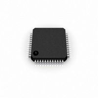
IC EMBEDDED USB HOST 48-LQFP
Manufacturer
Parallax Inc
Datasheet
1.604-00051.pdf
(17 pages)
Specifications of 604-00051
Controller Type
USB 2.0 Controller
Interface
UART
Voltage - Supply
3 V ~ 3.6 V
Current - Supply
25mA
Operating Temperature
0°C ~ 70°C
Mounting Type
Surface Mount
Package / Case
48-LQFP
Lead Free Status / RoHS Status
Lead free / RoHS Compliant
Available stocks
Company
Part Number
Manufacturer
Quantity
Price


2.2 Functional Block Descriptions
USB Host / Slave Transceivers 1 and 2 -
1.1 / USB 2.0 full�speed device interface. �n each the output drivers provide 3.3V level slew rate control signalling,
whilst a differential receiver and two single ended receivers provide USB data in, SE� and USB Reset condition
detection. These cells also incorporate internal USB pull�up or pull down resistors as required for host or slave mode.
USB Host / Slave Serial Interface Engine ( SIE ) -
conversion o� the USB Physical layer including bit su�fing � unstu�fing�� CRC generation � checking�� USB �rame
generation and error chec��ing.
12 MHz Oscillator -
from an e��teral 12�H�� crystal.
Clock Multiplier PLL -
and �8�H�� reference cloc�� signals, which is used by the USB SIE Bloc��s, the �CU core, System Timer and UART
Prescaler bloc��s.
Program and Test Logic -
is pulled low and the device is reset, the onboard E�Flash memory is bypassed by an internal hard coded BootStrap
Loader R�� which contains code to allow the E�Flash memory to be programmed via commands to the UART
interface. FTDI provides a software utility which allows the VNC1L to be programmed using this method. The TEST
pin is used in manufacturing to enhance the testability of the various internal bloc��s and should be tied to �ND.
DMA Controller 1 and 2 -
from the two USB SIE controllers, UART, FIF� and SPI to be transferred between each other via the data SRA� with
minimal �CU intervention.
Data SRAM -
accessed transparently to the �CU by the twin D�A controllers.
NPU ( Numeric CoProcessor ) -
transversing dis�� FAT tables which involve e��tensive 32 bit arithmetic. In order to speed up these operations, the �CU
has a dedicated 32 bit co�processor bloc��.
UART Prescaler -
value, the baud rate of the UART can be adjusted over a range of 300 baud to 1� baud.
SYSTEM TIMER -
is used by the �CU to provide timeouts and other timing functions.
VINCULUM MCU CORE -
�CU � E�CU ) architectiure. V�CU has a Harvard architecture i.e. separate code and data space and supports
6��� byes of program code, 6��� byes of � paged ) data space and 256 bytes of I� space. It uses “enhanced CISC”
technology � typically VNCU instructions would replace several lines of code in conventional CISC or RISC processors
giving RISC li��e performance in a CISC architecture with the advantage over both of e��cellent code compression in
the program R�� space.
E-FLASH Program ROM -
programming voltages are necessary for programming the onboard E�FLASH as these are provided internally on�chip.
Common methods of programming the E�FLASH � both under control of the V�CU ) are via the UART by pulling the
PR��# pin low and resetting the device �R by using the programming via a USB FLASH drive feature provided in
many o� the VNC1L firmware packages�
BOOTSTRAP LOADER ROM
e_FLASH memory when PR��# is pulled low. This provides a means of programming the entire E�Flash memory via
the UART interface.
UART and FIFO Logic
interfaces on FTDI’s FT232 and FT2�5 USB UART and FIF� products.
GPIO Blocks - general purpose IO pins� See the tables below to determine which are available �or any specific
configuration�
Vinculum VNC1L Embedded USB Host Controller I.C. Datasheet Version 0.95
This ��� �� 8bit bloc�� acts as the data � variable ) memory for the Vinculum �CU, though it can also be
The system timer provides a regular interrupt to the Vinculum �CU, typically at 1mS intervals. This
this bloc�� provides the master transmit / receive cloc�� for the UART bloc��. By varying the prescalar
The 12�H�� �scillator cell generates a 12�H�� reference cloc�� input to the Cloc�� �ultiplier PLL
-
The Cloc�� �ultiplier PLL ta��es the 12�H�� input from the �scillator Cell and generates 2��H��
These provide optional serial and parallel interfaces to the VNC1L equivalent to the
The twin D�A controllers in the VNC1L greatly enhance performance by allowing data
The “heart” of the VNC1L is the V�CU core based on FTDI’s proprietary 8�bit embedded
The VNCL1L has 6��� bytes of embedded Flash � E�Flash ) memory. No special
this bloc�� provides a means of programming the onboard E�Flash memory. When PR��#
-
This is a small bloc�� of hard encoded R�� � 512 �� 8 bits ) whivh bypasses the main
�ost Vinclum �CU operations are 8�bit, however there are some scenarios such as
The two USB transceiver cells provide the USB host / slave physical USB
These bloc��s handle the parallel to serial and serial to parallel
© Future Technology Devices International Ltd. 2006
Related parts for 604-00051
Image
Part Number
Description
Manufacturer
Datasheet
Request
R

Part Number:
Description:
IC ADC 12BIT 8CH MAX1270 24-DIP
Manufacturer:
Parallax Inc
Datasheet:

Part Number:
Description:
IC SENSOR TOUCH/PROXMTY 1CH 8DIP
Manufacturer:
Parallax Inc
Datasheet:


Part Number:
Description:
Microcontroller Modules & Accessories DISCONTINUED BY PARALLAX
Manufacturer:
Parallax Inc

Part Number:
Description:
BOOK UNDERSTANDING SIGNALS
Manufacturer:
Parallax Inc
Datasheet:


Part Number:
Description:
COMPETITION RING FOR SUMOBOT
Manufacturer:
Parallax Inc
Datasheet:


Part Number:
Description:
TEXT INFRARED REMOTE FOR BOE-BOT
Manufacturer:
Parallax Inc
Datasheet:
Part Number:
Description:
BOARD EXPERIMENT+LCD NX-1000
Manufacturer:
Parallax Inc
Datasheet:

Part Number:
Description:
CONTROLLER 16SERVO MOTOR CONTROL
Manufacturer:
Parallax Inc
Datasheet:

Part Number:
Description:
BASIC STAMP LOGIC ANALYZER
Manufacturer:
Parallax Inc
Datasheet: