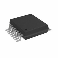
AD5933YRSZ Analog Devices Inc, AD5933YRSZ Datasheet - Page 32

AD5933YRSZ
Manufacturer Part Number
AD5933YRSZ
Description
IC NTWK ANALYZER 12B 1MSP 16SSOP
Manufacturer
Analog Devices Inc
Datasheet
1.AD5933YRSZ.pdf
(44 pages)
Specifications of AD5933YRSZ
Resolution (bits)
12 b
Master Fclk
16.776MHz
Voltage - Supply
2.7 V ~ 5.5 V
Operating Temperature
-40°C ~ 125°C
Mounting Type
Surface Mount
Package / Case
16-SSOP
Supply Voltage Range
2.7V To 5.5V
Operating Temperature Range
-40°C To +125°C
Digital Ic Case Style
SSOP
No. Of Pins
16
Frequency Max
0.1MHz
Termination Type
SMD
Pin Count
16
Screening Level
Automotive
Package Type
SSOP
Filter Terminals
SMD
Rohs Compliant
Yes
Communication Function
Network Analyzer
Lead Free Status / RoHS Status
Lead free / RoHS Compliant
For Use With
EVAL-AD5933EBZ - BOARD EVALUATION FOR AD5933
Tuning Word Width (bits)
-
Lead Free Status / Rohs Status
Compliant
Other names
AD5933BRSZ
Q2204656A
Q2204656A
Available stocks
Company
Part Number
Manufacturer
Quantity
Price
Company:
Part Number:
AD5933YRSZ
Manufacturer:
ADI
Quantity:
5 000
Company:
Part Number:
AD5933YRSZ
Manufacturer:
Fujitsu
Quantity:
500
Part Number:
AD5933YRSZ
Manufacturer:
ADI/亚德诺
Quantity:
20 000
AD5933
The key point is that the output impedance of the external
amplifier in Figure 41 (which is also in series with Z
has a far less significant effect on gain factor calibration and
subsequent impedance readings in comparison to connecting
the small impedance directly to the VOUT pin (and directly in
series with R
impedance from the effects of R
output impedance in series with Z
For example, if the user measures Z
have a small impedance value within the range of 90 Ω to
110 Ω over the frequency range of 30 kHz to 32 kHz, the
user may not be in a position to measure R
the factory/lab. Therefore, the user may choose to add on
an extra amplifier circuit like that shown in Figure 41 to the
signal path of the AD5933. The user must ensure that the
chosen external amplifier has a sufficiently low output series
resistance over the bandwidth of interest in comparison to the
impedance range under test (for an op amp selection guide, see
www.analog.com/opamps). Most amplifiers from Analog
Devices have a curve of closed loop output impedance vs.
frequency at different amplifier gains to determine the output
series impedance at the frequency of interest.
The system settings are
VDD = 3.3 V
VOUT = 2 V p-p
R2 = 20 kΩ
R1 = 4 kΩ
Gain setting resistor = 500 Ω
Z
PGA setting = ×1
UNKNOWN
OUT
= 100 Ω
). The external amplifier buffers the unknown
OUT
UNKNOWN
and introduces a smaller
UNKNOWN
.
OUT
that is known to
directly in
UNKNOWN
)
Rev. C | Page 32 of 44
To attenuate the excitation voltage at VOUT, choose a ratio
of R1/R2. With the values of R1 = 4 kΩ and R2 = 20 kΩ,
attenuate the signal by 1/5
maximum current flowing through the impedance is 400 mV/
90 Ω = 4.4 mA.
The system is subsequently calibrated using the usual method
with a midpoint impedance value of 100 Ω, a calibration
resistor, and a feedback resistor at a midfrequency point in the
sweep. The dynamic range of the input signal to the receive side
of the AD5933 can be improved by increasing the value of the
I-V gain resistor at the RFB pin. For example, increasing the I-V
gain setting resistor at the RFB pin increases the peak-to-peak
signal presented to the ADC input from 400 mV (RFB = 100 Ω)
to 2 V p-p (RFB = 500 Ω).
The gain factor calculated is for a 100 Ω resistor connected
between VOUT and VIN, assuming the output series resistance
of the external amplifier is small enough to be ignored.
When biasing the circuit shown in Figure 41, note that the
receive side of the AD5933 is hard-biased about VDD/2 by
design. Therefore, to prevent the output of the external
amplifier (attenuated AD5933 Range 1 excitation signal) from
saturating the receive side amplifiers of the AD5933, a voltage
equal to VDD/2 must be applied to the noninverting terminal
of the external amplifier.
th
of 2 V p-p = 400 mV. The


