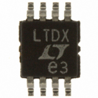
LTC1484CMS8#PBF Linear Technology, LTC1484CMS8#PBF Datasheet

LTC1484CMS8#PBF
Specifications of LTC1484CMS8#PBF
Available stocks
Related parts for LTC1484CMS8#PBF
LTC1484CMS8#PBF Summary of contents
Page 1
... IEC-1000-4-2 level 4 ( 8kV) contact and level 3 ( 8kV) air discharge ESD without latchup or damage. The LTC1484 is fully specified over the commercial and industrial temperature ranges and is available in 8-lead MSOP, PDIP and SO packages. , LTC and LT are registered trademarks of Linear Technology Corporation. LTC1484 V RO2 CC2 B2 ...
Page 2
LTC1484 ABSOLUTE MAXIMUM (Note 1) Supply Voltage (V )............................................... 6.5V CC Control Input Voltages ................. – 0. Driver Input Voltage ..................... – 0. Driver Output Voltages ................................. – 10V Receiver Input ...
Page 3
ELECTRICAL CHARACTERISTICS temperature range, otherwise specifications are at T SYMBOL PARAMETER V Receiver Input Hysteresis TH V Receiver Output High Voltage OH V Receiver Output Low Voltage OL I Three-State (High Impedance) Output Current OZR at Receiver R Receiver Input ...
Page 4
LTC1484 U SWITCHING CHARACTERISTICS temperature range, otherwise specifications are at T SYMBOL PARAMETER t Driver Enable from Shutdown to Output High ZH(SHDN) t Driver Enable from Shutdown to Output Low ZL(SHDN) t Receiver Enable from Shutdown to Output High ZH(SHDN) ...
Page 5
W U TYPICAL PERFOR A CE CHARACTERISTICS Receiver Input Offset Voltage vs Temperature –20 –40 –60 –80 –100 V = –7V CM –120 –140 V = 12V CM –160 –180 –200 ...
Page 6
LTC1484 W U TYPICAL PERFOR A CE CHARACTERISTICS Receiver Short-Circuit Current vs Temperature 100 V = 5.25V OUTPUT LOW 60 SHORT OUTPUT HIGH 20 SHORT TO GROUND 10 0 –55 ...
Page 7
W U TYPICAL PERFOR A CE CHARACTERISTICS Driver Differential Output Voltage vs Temperature 3 2.5 2 5.25V 1 4.75V 4.5V 1.0 CC 0.5 V ...
Page 8
LTC1484 W U TYPICAL PERFOR A CE CHARACTERISTICS Driver Output High Voltage vs Output Current 5 4.75V CC 4.5 4.0 3.5 3.0 2.5 2.0 1.5 1.0 0.5 0 –100 –90 –80 –70 –60 –50 –40 –30 –20 –10 ...
Page 9
PIN FUNCTIONS A (Pin 6): Driver Output/Receiver Input. The input resis- tance is typically 22k when the driver is disabled (DE = 0). When the driver is enabled, the A output follows the logic level at the ...
Page 10
LTC1484 U W SWITCHI WAVEFOR 1. 90% 10% – 1 NOTE 1. 2.3V ...
Page 11
U W SWITCHI WAVEFOR DZR V(A) – V(B) RO NOTE AND B ARE THREE-STATED WHEN APPLICATIONS INFORMATION Low Power ...
Page 12
LTC1484 U U APPLICATIONS INFORMATION Shutdown Mode The receiver output (RO) and the driver outputs (A, B) can be three-stated by taking the RE and DE pins high and low respectively. Taking RE high and DE low at the same ...
Page 13
U U APPLICATIONS INFORMATION 5V 5V 1.2k 120 8 5V 1.2k 1k receiver output and expects to see perfect agreement between the two data streams. (Note that the driver inverts the data, so the transmitted and received data streams are ...
Page 14
LTC1484 U U APPLICATIONS INFORMATION longer delay for the falling edge is due to the larger voltage range the line must swing (typically > 2V compared to 370mV) before the receiver trips high again. The differ- ence in delay affects ...
Page 15
... FLASH SHALL NOT EXCEED 0.010" (0.254mm) PER SIDE Information furnished by Linear Technology Corporation is believed to be accurate and reliable. However, no responsibility is assumed for its use. Linear Technology Corporation makes no represen- tation that the interconnection of its circuits as described herein will not infringe on existing patent rights. ...
Page 16
... Highest Input Impedance, Low EMI, Lowest Power 2500V Propagation Delay Skew 500ps (Typ) Low Power, 15kV ESD Protection “A” “B” 1484 TA02 Isolation RMS 15kV ESD Protection, Industry Standard Pinout 1484f LT/TP 0400 4K • PRINTED IN USA LINEAR TECHNOLOGY CORPORATION 1998 ...


