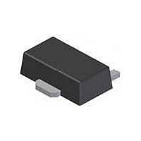
AP1115BY50L-13 Diodes Inc, AP1115BY50L-13 Datasheet - Page 4

AP1115BY50L-13
Manufacturer Part Number
AP1115BY50L-13
Description
Low Dropout (LDO) Regulators LDO BI 0.6A 1.3V 12V 1.25V 5.0V FIX
Manufacturer
Diodes Inc
Datasheet
1.AP1115BY18L-13.pdf
(8 pages)
Specifications of AP1115BY50L-13
Number Of Outputs
1
Polarity
Positive
Input Voltage Max
18 V
Output Voltage
5 V
Output Type
Fixed
Dropout Voltage (max)
1.3 V at 600 mA
Output Current
600 mA
Line Regulation
0.2 %
Load Regulation
50 mV
Maximum Power Dissipation
5 W
Maximum Operating Temperature
+ 150 C
Mounting Style
SMD/SMT
Package / Case
SOT-89-3L
Minimum Operating Temperature
0 C
Lead Free Status / Rohs Status
Lead free / RoHS Compliant
Available stocks
Company
Part Number
Manufacturer
Quantity
Price
Part Number:
AP1115BY50L-13
Manufacturer:
DIODES/美台
Quantity:
20 000
Part Number:
AP1115BY50L-13R
Manufacturer:
DIODES/美台
Quantity:
20 000
Electrical Characteristics
Notes:
AP1115
Document number: DS31026 Rev. 8 - 2
Load Regulation
Dropout Voltage
(V
Current Limit
Current (Note 4)
Thermal Regulation
Ripple Rejection
Temperature Stability I
Minimum Load
IN
-V
Parameter
OUT
2. See thermal regulation specifications for changes in output voltage due to heating effects. Line and load regulation are measured at a constant
3. Line and load regulation are guaranteed up to the maximum power dissipation of 5W. Power dissipation is determined by the input/output differential
4. Quiescent current is defined as the minimum output current required to maintain regulation. At 12V input/output differential the device is guaranteed
5. Test conditions for SOT89-3L: Device mounted on FR-4 substrate, 2oz copper, with minimum recommended pad layout.
θ
θ
)
JC
JA
and the output current. Guaranteed maximum power dissipation will not be available over the full input/output range.
to regulate if the output current is greater than 10mA.
junction temperature by low duty cycle pulse testing. Load regulation is measured at the output lead = 1/18” from the package.
AP1115-ADJ
AP1115-1.5
AP1115-1.8
AP1115-2.5
AP1115-2.8
AP1115-3.0
AP1115-3.3
AP1115-3.5
AP1115-5.0
AP1115-ADJ/1.5/1.8
2.5/2.8/3.0/3.3/3.5/5.0
AP1115-ADJ/1.5/1.8
2.5/2.8/3.0/3.3/3.5/5.0
AP1115-XXX
T
f = 120Hz,C
AP1115-XXX
Thermal Resistance Junction-to-Ambient
(No heat sink; No air flow) (Note 5)
Thermal Resistance Junction-to-Case
Control Circuitry/Power Transistor (Note 5)
O
A
= 10mA
= 25
o
C, 30ms pulse
OUT
(under operating conditions) (cont.)
= 25uF Tantalum, I
Conditions
V
T
V
T
V
T
V
T
V
T
V
T
V
T
V
T
V
T
I
(V
0
V
OUT
A
A
A
A
A
A
A
A
A
o
IN
IN
IN
IN
IN
IN
IN
IN
IN
IN
C ≤ T
IN
= 25
= 25
= 25
= 25
= 25
= 25
= 25
= 25
= 25
= 3.3V, V
= 3V, 0mA < Io < 0.6A,
= 3.3V, 0mA < Io < 0.6A,
= 4V, 0mA < Io < 0.6A,
= 4.3V, 0mA < Io < 0.6A,
= 5V, 0 ≤ I
= 5V, 0 ≤ I
= 5V, 0 ≤ I
= 8V, 0 ≤ I
= V
-V
= 0.6A, ΔV
0.6A LOW DROPOUT POSITIVE ADJUSTABLE OR
www.diodes.com
OUT
o
o
o
o
o
o
o
o
o
OUT
J
C (Note 2, 3)
C (Note 2, 3)
C (Note 2, 3)
C (Note 2, 3)
C (Note 2, 3)
C (Note 2, 3)
C (Note 2, 3)
C (Note 2, 3)
C (Note 2, 3)
≤ 125
) = 5V
OUT
+3V
4 of 8
ADJ
OUT
OUT
OUT
OUT
= 0.6A
o
OUT
C
= 0,0mA < Io < 0.6A,
≤ 0.6A,
≤ 0.6A,
≤ 0.6A,
≤ 0.6A,
= 1%V
OUT
FIXED-MODE REGULATOR
Min
0.7
-
-
-
-
-
-
-
-
-
-
-
-
-
-
-
-
0.008
Typ.
164
1.1
0.6
12
15
20
22
23
26
28
40
60
35
5
-
-
AP1115
Max
0.04
© Diodes Incorporated
1.3
15
18
25
28
30
33
35
50
10
70
1
-
-
-
-
April 2011
o
o
%/W
Unit
mV
mV
mV
mV
mV
mV
mV
mV
mA
C/W
C/W
dB
%
%
V
A


