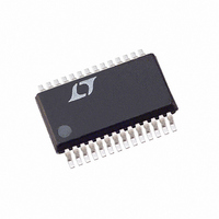
LTC2844CG#PBF Linear Technology, LTC2844CG#PBF Datasheet - Page 6

LTC2844CG#PBF
Manufacturer Part Number
LTC2844CG#PBF
Description
IC TXRX 3.3V MULTIPROTCOL 28SSOP
Manufacturer
Linear Technology
Type
Transceiverr
Datasheet
1.LTC2844CGPBF.pdf
(20 pages)
Specifications of LTC2844CG#PBF
Number Of Drivers/receivers
4/4
Protocol
Multiprotocol
Voltage - Supply
3.3V
Mounting Type
Surface Mount
Package / Case
28-SSOP
Lead Free Status / RoHS Status
Lead free / RoHS Compliant
Available stocks
Company
Part Number
Manufacturer
Quantity
Price
PI FU CTIO S
LTC2844
6
V
to V
capacitor to ground.
V
V
capacitor to ground.
D1 (Pin 3): TTL Level Driver 1 Input.
D2 (Pin 4): TTL Level Driver 2 Input.
D3 (Pin 5): TTL Level Driver 3 Input.
R1 (Pin 6): CMOS Level Receiver 1 Output. Receiver
outputs have a weak pull up to V
R2 (Pin 7): CMOS Level Receiver 2 Output.
R3 (Pin 8): CMOS Level Receiver 3 Output.
D4 (Pin 9): TTL Level Driver 4 Input.
R4 (Pin 10): CMOS Level Receiver 4 Output.
M0 (Pin 11): TTL Level Mode Select Input 0. Mode select
inputs pull up to V
M1 (Pin 12): TTL Level Mode Select Input 1.
M2 (Pin 13): TTL Level Mode Select Input 2.
DCE/DTE (Pin 14): TTL Level Mode Select Input.
CC
DD
DD
U
(Pin 1): Positive Supply for the Transceivers. Connect
CC
(Pin 2): Positive Supply Voltage for V.28. Connect to
Pin 7 on LTC2846 or 8V supply. Connect a 1 F
Pin 8 on LTC2846 or to 5V supply. Connect a 1 F
U
IN
U
.
IN
when high impedance.
V
3V V
D4/R4 A (Pin 16): Receiver 4 Inverting Input and Driver 4
Inverting Output.
R3 B (Pin 17): Receiver 3 Noninverting Input.
R3 A (Pin 18): Receiver 3 Inverting Input.
R2 B (Pin 19): Receiver 2 Noninverting Input.
R2 A (Pin 20): Receiver 2 Inverting Input.
D3/R1 B (Pin 21): Receiver 1 Noninverting Input and
Driver 3 Noninverting Output.
D3/R1 A (Pin 22): Receiver 1 Inverting Input and Driver 3
Inverting Output.
D2 B (Pin 23): Driver 2 Noninverting Output.
D2 A (Pin 24): Driver 2 Inverting Output.
D1 B (Pin 25): Driver 1 Noninverting Output.
D1 A (Pin 26): Driver 1 Inverting Output.
GND (Pin 27): Ground.
V
Pin 31 on LTC2846 or to – 7V supply. Connect a 1 F
capacitor to ground.
IN
EE
(Pin 15): Positive Supply for the Receiver Outputs.
(Pin 28): Negative Supply Voltage. Connect to V
IN
3.6V. Connect a 1 F capacitor to ground.
sn2844 2844fs
EE


