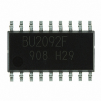
BU2092F-E2 Rohm Semiconductor, BU2092F-E2 Datasheet - Page 19

BU2092F-E2
Manufacturer Part Number
BU2092F-E2
Description
IC DRIVER 12BIT S-IN P-OUT SOP18
Manufacturer
Rohm Semiconductor
Type
Driverr
Specifications of BU2092F-E2
Number Of Drivers/receivers
12/0
Voltage - Supply
2.7 V ~ 5.5 V
Mounting Type
Surface Mount
Package / Case
18-SOP
Output Current
25mA
No. Of Outputs
12
Supply Voltage Range
2.7V To 5.5V
Driver Case Style
SOP
No. Of Pins
18
Operating Temperature Range
-20°C To +75°C
Svhc
No SVHC (18-Jun-2010)
Base
RoHS Compliant
Supply Voltage (max)
5.5 V
Supply Voltage (min)
2.7 V
Supply Current
0.025 A
Maximum Operating Temperature
+ 75 C
Mounting Style
SMD/SMT
Minimum Operating Temperature
- 25 C
Output Voltage
2 V to 1 V
Base Number
2092
Rohs Compliant
Yes
Lead Free Status / RoHS Status
Lead free / RoHS Compliant
Protocol
-
Lead Free Status / Rohs Status
Lead free / RoHS Compliant
Other names
BU2092F-E2TR
Available stocks
Company
Part Number
Manufacturer
Quantity
Price
Part Number:
BU2092F-E2
Manufacturer:
ROHM/罗姆
Quantity:
20 000
【BU2152FS】
●Pin descriptions
●Timing chart
© 2009 ROHM Co., Ltd. All rights reserved.
BU2050F,BU2092F,BU2092FV,BU2099FV,BD7851FP,BU2152FS
www.rohm.com
5 ~ 28
CLK
DATA
STB
Pn
SO
No.
Pin
29
30
31
32
1
2
3
4
1.
2.
3.
4.
[ Truth Table ]
CLK
H
×
L
After the power is turned on and the voltage is stabilized, STB should be activated, after clocking 24 data bits into
the DATA terminal.
Pn parallel output data of the shift register is set after the 24
Since the STB is a label latch, data is retained in the “H” section and renewed in the “L” section of the STB.
The final stage data of the shift register is outputted to the SO by synchronizing with the rise time of the CLOCK.
Pin Name
P1 ~ P24
DATA
CLK
STB
CLB
V
V
V
SO
DD
SS
SS
DATA24
Input
STB
H
×
L
Previous
DATA24
I/O
DATA23
O
O
-
I
-
I
I
I
-
CLB
H
H
L
Previous
DATA23
Previous DATA
Clock Input
Cascade Output
Function
Ground
Ground
Serial Data Input
Parallel Data Output
Strobe Signal Input active “L”
Clear Signal Input active “L”
Power Supply
DATA22
All the data of the latch circuit are set to “H” (data of shift register does not
change), all the parallel outputs are “H”.
Serial data of DATA pin are latched to the shift register.
At this time, the data of the latch circuit does not change.
The data of the shift register are transferred to the latch circuit, and the data of
the latch circuit are outputted from the parallel output pin.
The data of the shift register shifts 1bit, and the data of the latch circuit and
parallel output also change.
Fig. 18
19/24
Previous
DATA2
th
clock by the LCK.
DATA2
Function
Previous
DATA1
DATA1
DATA24
DATA23
Technical Note
2009.06 - Rev.A
DATA
DATA22


