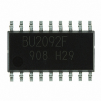
BU2092F-E2 Rohm Semiconductor, BU2092F-E2 Datasheet - Page 7

BU2092F-E2
Manufacturer Part Number
BU2092F-E2
Description
IC DRIVER 12BIT S-IN P-OUT SOP18
Manufacturer
Rohm Semiconductor
Type
Driverr
Specifications of BU2092F-E2
Number Of Drivers/receivers
12/0
Voltage - Supply
2.7 V ~ 5.5 V
Mounting Type
Surface Mount
Package / Case
18-SOP
Output Current
25mA
No. Of Outputs
12
Supply Voltage Range
2.7V To 5.5V
Driver Case Style
SOP
No. Of Pins
18
Operating Temperature Range
-20°C To +75°C
Svhc
No SVHC (18-Jun-2010)
Base
RoHS Compliant
Supply Voltage (max)
5.5 V
Supply Voltage (min)
2.7 V
Supply Current
0.025 A
Maximum Operating Temperature
+ 75 C
Mounting Style
SMD/SMT
Minimum Operating Temperature
- 25 C
Output Voltage
2 V to 1 V
Base Number
2092
Rohs Compliant
Yes
Lead Free Status / RoHS Status
Lead free / RoHS Compliant
Protocol
-
Lead Free Status / Rohs Status
Lead free / RoHS Compliant
Other names
BU2092F-E2TR
Available stocks
Company
Part Number
Manufacturer
Quantity
Price
Part Number:
BU2092F-E2
Manufacturer:
ROHM/罗姆
Quantity:
20 000
•
•
Q0 to Q11 output for the BU2090 / F / FS and BU2092 / F / FV is Nch open drain output. When the shift register transfer data is LOW,
the corresponding output FET is ON (continuous state). When the transfer data is HIGH, the output FET is OFF (discontinuous).
CLOCK DATA
Pin No.
Standard ICs
Truth table
Input / output circuit
BU2092 / F / FV
BU2090 / F / FS
H
L
INPUT
2, 3
LCK
V
DD
GND (V
Pin No.
BU2092 / F
SS
OE
H
L
)
2, 3, 4, 17
Output (Q0 to Q11) disabled
Output (Q0 to Q11) enabled
First cell of the shift register stores the LOW. Other cells, respectively, store
data from the preceding cells or other prior data. (Output state is HOLD.)
First cell of the shift register stores the HIGH. Other cells, respectively, store
data from the preceding cells or other prior data. (Storage state and output state are HOLD.)
No change in shift register.
Contents of shift register are stored in storage register.
No change in shift register.
V
GND (V
DD
SS
Pin No.
)
BU2092FV
2, 3, 4, 19
Pin No.
BU2090 / F / FS
4, 5, 6, 7, 8, 9
10, 11, 12, 13
14, 15
FUNCTION
BU2090 / BU2090F / BU2090FS /
Pin No.
BU2092 / BU2092F / BU2092FV
BU2092 / F
GND (V
10, 11, 12, 13
14, 15, 16
5, 6, 7, 8, 9,
SS
)
Pin No.
BU2092FV
10, 11, 14, 15
5, 6, 7, 8, 9,
16, 17, 18
7


