MIC3001GML Micrel Inc, MIC3001GML Datasheet
MIC3001GML
Specifications of MIC3001GML
MIC3001GML
Available stocks


Related parts for MIC3001GML

MIC3001GML Summary of contents
Page 1
... MLF and MicroLeadFrame are registered trademarks of Amkor Technology. Micrel Inc. • 2180 Fortune Drive • San Jose, CA 95131 • USA • tel +1 (408) 944-0800 • fax + 1 (408) 474-1000 • http://www.micrel.com August 2004 FOM Management IC with Internal ...
Page 2
... Ordering Information Part Number Package Type MIC3001BML 24-pin MLF (1) MIC3001BMLTR 24-pin MLF MIC3001GML 24-pin MLF (1) MIC3001GMLTR 24-pin MLF Note: 1. Tape and Reel. August 2004 Junction Temp. Range ® –45°C to +105°C ® –45°C to +105°C ® –45°C to +105°C ® ...
Page 3
Micrel, Inc. Contents General Description ...................................................................................................................................................... 1 Applications................................................................................................................................................................... 1 Ordering Information .................................................................................................................................................... 2 Pin Configuration .......................................................................................................................................................... 7 Pin Description .............................................................................................................................................................. 7 Absolute Maximum Ratings ......................................................................................................................................... 9 Operating Ratings ......................................................................................................................................................... 9 Electrical Characteristics ............................................................................................................................................. 9 Timing Diagram ........................................................................................................................................................... 14 Address Map................................................................................................................................................................ ...
Page 4
Micrel, Inc. Alarm Flags.................................................................................................................................................................. 52 Warning Flags.............................................................................................................................................................. 53 Applications Information............................................................................................................................................ 69 Controlling Laser Diode Bias..................................................................................................................................... 69 Choosing C ........................................................................................................................................................ 70 COMP Measuring Laser Bias Current .................................................................................................................................. 70 Interfacing To Laser Drivers...................................................................................................................................... 70 SY88912 3.3V 3.2Gbps SONET/SDH Laser Driver ................................................................................................. 71 ...
Page 5
Micrel, Inc. List of Figures Figure 1. MIC3001 Block Diagram ...................................................................................................................................................17 Figure 2. Analog-to-Digital Converter Block Diagram.......................................................................................................................18 Figure 3. RXPOT Block Diagram .....................................................................................................................................................22 Figure 4. MIC3001 APC and Modulation Control Block Diagram ....................................................................................................22 Figure 5. Programmable Feedback Resistor....................................................................................................................................22 Figure 6. ...
Page 6
Micrel, Inc. List of Tables Table 1. MIC3001 Address Map, Serial Address = A0 Table 2. MIC3001 Address Map, Serial Address = A2 Table 3. Temperature Compensation Tables, Serial Address = A4 Table 4. OEM Configuration Registers, Serial Address = ...
Page 7
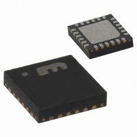
Micrel, Inc. Pin Configuration Pin Description Pin Number Pin Name VMPD 3 GNDA 4 VDDA 5 VILD– 6 VILD+ 7 SHDN (TXFIN) 8 SHDN (TXFIN) 9 XPN 10 TXFAULT August 2004 24-Pin MLF® Pin Function Analog Input. ...
Page 8
Micrel, Inc. Pin Description Pin Number Pin Name Pin Function 11 TXDISABLE Digital Input; Active High. The transmitter is disabled when this line is high or the STXDIS bit is set. The state of this input is always reflected in ...
Page 9
Micrel, Inc. Absolute Maximum Ratings Power Supply Voltage, V ................................. +3.8V DD Voltage on CLK, DATA, TXFAULT, VIN, RXLOS, DISABLE, RSIN................................. –0.3V to +6.0V Voltage On Any Other Pin...............–0. Power Dissipation 85°C ............................... 1.5W A Junction ...
Page 10
Micrel, Inc. Voltage-to-Digital Converter Characteristics ( AUX , V BIAS , V MPD , V ILD ±) Symbol Parameter Voltage Measurement Error t Conversion Time CONV t Sample Period SAMPLE Voltage Input, V (Pin 14 used as ...
Page 11
Micrel, Inc. Electrical Characteristics Symbol Parameter V MOD Buffer Op-Amp, V MOD +, V MOD – GBW Gain Bandwidth TC Input Offset Voltage VOS Temperature Coefficient I V – Input Current BIAS MOD V Output Voltage Swing OUT I Output ...
Page 12
Micrel, Inc. Electrical Characteristics Symbol Parameter Control and Status I/O Timing, TXFAULT, TXDISABLE, RSIN, RSOUT, and RXLOS t TXDISABLE Assert Time OFF t TXDISABLE De-assert Time ON t Initialization Time INIT t Power-on Initialization Time INIT2 t TXFAULT Assert Time ...
Page 13
Micrel, Inc. Serial Data I/O Pin, Data Symbol Parameter V Low Output Voltage OL V Low Input Voltage IL V High Input Voltage IH I Input Current LEAK C Input Capacitance IN Serial Clock Input, CLK V Low Input Voltage ...
Page 14
Micrel, Inc. Timing Diagram August 2004 Serial Interface Timing 14 hbwhelp@micrel.com MIC3001 M9999-082404-A or (408) 955-1690 ...
Page 15
Micrel, Inc. Address Map Address(s) Field Size Name (Bytes) 0 –95 96 Serial ID defined by SEP MSA 96 – 127 32 Vendor Specific 128 – 255 128 Reserved Table 1. MIC3001 Address Map, Serial Address = A0 Address(s) Field ...
Page 16
Micrel, Inc. Address(s) Field Size (Bytes) HEX DEC ...
Page 17
Micrel, Inc. Block Diagram MIC3000 Capability In general, the MIC3001 is completely hardware and software backward compatible with the MIC3000. Every feature available in the MIC3000 is still present in the MIC3001. New features have, of course, been added. The ...
Page 18
ADC Resolution Channel (bits) TEMP 8 VAUX 8 VMPD 8 VILD 8 VRX 12 Note: 1. Assumes typical VREF value of 1.22V. Channel DDA V BIAS V MOD APCDAC MODDAC FLTDAC Note: 1. Assumes typical V August ...
Page 19
Micrel, Inc. Internal/External Calibration The default mode of calibration in the MIC3001 is external calibration, for which INTCAL bit (bit 0 in OEMCF3 register) is set to 0. This mode is backward compatible with MIC3000. The internal calibration mode is ...
Page 20
Micrel, Inc. RX Power Received power is sensed as a voltage appearing at VRX assumed that this voltage is generated by a sense resistor carrying the receiver photodiode current. For a given implementation, the constant, K, will likely ...
Page 21
Micrel, Inc. Address(s) Field Size HEX DEC 48-49 72-73 2 RESERVED 4A-4B 74-75 2 TOFFh:TOFFl 4C-4D 76-77 2 VSLPh:VSLPl 4E-4F 78-79 2 VOFFh:VOFFl 50-61 80-81 2 ISLPh:ISLPl 52-63 82-83 2 IOFFh:IOFFl 54-65 84-85 2 TXSLPh: TXSLPl 56-67 86-87 2 TXOFFh: ...
Page 22
Micrel, Inc. C/ ADC Result Registers Reading In the present revision of MIC3001, the ADC result registers should be read as 16 bit registers under internal calibration while under external calibration they should be read as 8 bit registers at ...
Page 23
Micrel, Inc. Laser Modulation Control As shown in Figure 4, a temperature-compensated DAC is provided to set and control the laser modulation current via an external laser driver circuit. MODREF in OEMCFG0 selects whether the V MOD up from ground ...
Page 24
Micrel, Inc. Power ON and Laser Start-Up When power is applied, the MIC3001 initializes its internal registers and state machine. This process takes t POR , about 50ms. Following t POR , analog-to-digital conversions begin, serial communication is possible, and ...
Page 25
Micrel, Inc. Fault Comparators In addition to detecting and reporting the events specified in SFF-8472, the MIC3001 also monitors five fault conditions: inadequate supply voltage, thermal diode faults, excessive bias current, excessive transmit power, and APC op-amp saturation. Comparators monitor ...
Page 26
Micrel, Inc. the fault comparators. Since laser bias current varies greatly with temperature, there is a temperature compensation look-up table for the bias current fault DAC value. When a fault condition is detected, the laser will be immediately shutdown and ...
Page 27
Micrel, Inc. performed using a look-up table (LUT) that stores values corresponding to each measured temperature over a 128°C span. Four identical tables reside at serial address A4h as summarized in Table 13. The range of temperatures spanned by the ...
Page 28
Micrel, Inc. Register Table Offset Address 00h 0 01h 1 02h 2 • • • • • • 3Eh 62 3Fh 63 Table 14. APC Temperature Compensation Look-Up Table, Serial Address 12C ADR+4 Register Table Offset Address 40h 0 41h ...
Page 29
Micrel, Inc. The LUTOFF register determines the range of measured temperatures that are actually spanned by the tables. The temperature span of the tables versus the value of LUTOFF is given in Table 18. LUTOFF Temperature Span t (min) – ...
Page 30
Micrel, Inc. August 2004 Figure 13. Temperature Compensation Examples 30 MIC3001 M9999-082404-A hbwhelp@micrel.com or (408) 955-1690 ...
Page 31
Micrel, Inc. Alarms and Warning Flags There are twenty different conditions that will cause the MIC3001 to set one of the bits in the WARNx or ALARMx registers. These conditions are listed in Table 19. The less critical of these ...
Page 32
Micrel, Inc. System Timing The timing specifications for MIC3001 control and status I/O are given in the “Electrical Characteristics” section. Figure 16. Initialization Timing with TXDISABLE Asserted August 2004 Figure 14. Control and Status I/O Logic Figure 15. Transmitter ON-OFF ...
Page 33
Micrel, Inc. Figure 17. Initialization Timing with TXDISABLE Not Asserted August 2004 Figure 18. Loss-of-Signal (LOS) Timing Figure 19. Transmit Fault Timing 33 MIC3001 M9999-082404-A hbwhelp@micrel.com or (408) 955-1690 ...
Page 34
Micrel, Inc. August 2004 Figure 20. Successfully Clearing a Fault Condition Figure 21. Unsuccessful Attempt to Clear a Fault 34 MIC3001 M9999-082404-A hbwhelp@micrel.com or (408) 955-1690 ...
Page 35
Micrel, Inc. Warm Resets The MIC3001 can be reset to its power-on default state during operation by setting the reset bit in OEMCFG0. When this bit is set, TXFAULT and RXLOS will be de- asserted, all registers will be restored ...
Page 36
Micrel, Inc. Serial Port Operation The MIC3001 uses standard Write_Byte, Read_Byte, and Read_Word operations for communication with its host. It also supports Page_Write and transactions. The Write_Byte operation involves sending the device’s slave address (with the R/W bit low to ...
Page 37
Micrel, Inc. Acknowledge Polling The MIC3001’s non-volatile memory cannot be accessed during the internal write process. To allow for maximum speed bulk writes, the MIC3001 supports acknowledge polling. The MIC3001 will not acknowledge serial bus transactions while internal writes are ...
Page 38
Micrel, Inc. Detailed Register Descriptions Note: Serial bus addresses shown assume that I2CADR = Ax Alarm Threshold Registers D[7] D[6] read/write read/write read/write Default Value Serial Address Byte Address Each LSB represents one degree centigrade. This register ...
Page 39
Micrel, Inc. D[7] D[6] read/write read/write read/write Default Value Serial Address Byte Address Each LSB represents 25.6mV. This register used in conjunction with VMAXl to yield a sixteen-bit value. The value in TMINh is compared against VINh. ...
Page 40
Micrel, Inc. D[7] D[6] read/write read/write read/write Default Value Serial Address Byte Address This register used in conjunction with IMAXl to yield a sixteen-bit value. The value in this register is uncalibrated. The value in IMAXh is ...
Page 41
Micrel, Inc. D[7] D[6] read/write read/write read/write Default Value Serial Address Byte Address Each LSB represents 25.6µW. This register used in conjunction with TXOPl to yield a sixteen-bit value. The values in TXOPh:TXOPl are in an unsigned ...
Page 42
Micrel, Inc. RX Optical Power High Alarm Threshold MSB (RXMAXh) D[7] D[6] read/write read/write read/write Default Value Serial Address Byte Address Each LSB represents 25.6µW. This register used in conjunction with RXMAXl to yield a sixteen-bit value. ...
Page 43
Micrel, Inc. Warning Threshold Registers Temperature High Warning Threshold MSB (THIGHh) D[7] D[6] read/write read/write read/write Default Value Serial Address Byte Address Each LSB represents one degree centigrade. This register used in conjunction with THIGHl to yield ...
Page 44
Micrel, Inc. D[7] D[6] read/write read/write read/write Default Value Serial Address Byte Address Each LSB represents 25.6mV. This register used in conjunction with VHIGHl to yield a sixteen-bit value. The value in this register is uncalibrated. The ...
Page 45
Micrel, Inc. Bias Current High Warning Threshold MSB (IHIGHh) D[7] D[6] read/write read/write read/write Default Value Serial Address Byte Address This register used in conjunction with IHIGHl to yield a sixteen-bit value. The value in this register ...
Page 46
Micrel, Inc. D[7] D[6] read/write read/write read/write Default Value Serial Address Byte Address Each LSB represents 25.6µW. This register used in conjunction with TXHIGHl to yield a sixteen-bit value. The values in TXHIGHh:TXHIGHl are in an unsigned ...
Page 47
Micrel, Inc. RX Optical Power High Warning Threshold MSB (RXHIGHh) D[7] D[6] read/write read/write read/write Default Value Serial Address Byte Address Each LSB represents 25.6µW. This register used in conjunction with RXHIGHl to yield a sixteen-bit value. ...
Page 48
Micrel, Inc. D[7] D[6] read/write read/write read/write Default Value Serial Address Byte Address This register is provided for compliance with SFF-8472 implemented as general-purpose non-volatile memory. Read/write access is possible whenever a valid OEM password has been entered. ...
Page 49
Micrel, Inc. ADC Result Registers D[7] D[6] read-only read-only read-only Default Value Serial Address Byte Address Each LSB represents one degree centigrade. This register used in conjunction with TEMPl to yield a sixteen-bit temperature value. The value ...
Page 50
Micrel, Inc. D[7] D[6] read-only read-only read-only Default Value Serial Address Byte Address This register used in conjunction with ILDl to yield a sixteen-bit value. The values in ILDh:ILDl are in an unsigned binary format. The value ...
Page 51
Micrel, Inc. D[7] D[6] read-only read-only read-only Default Value Serial Address Byte Address Each LSB represents 25.6µW. This register used in conjunction with RXOPl to yield a sixteen-bit value. The values in RXOPh:RXOPl are in an unsigned ...
Page 52
Micrel, Inc. Alarm Flags D[7] D[ read-only read-only read-only Default Value Serial Address Byte Address The power-up default value Following the first A/D conversion, however, any of the bits may be set depending on ...
Page 53
Micrel, Inc. Warning Flags D[7] D[ read-only read-only read-only Default Value Serial Address Byte Address The power-up default value Following the first A/D conversion, however, any of the bits may be set depending on ...
Page 54
Micrel, Inc. D[7] D[6] read/write read/write read/write Default Value Serial Address Byte Address This four-byte field is for entry of the password required to access the OEM area of the MIC3001’s memory and registers. A valid OEM password will also ...
Page 55
Micrel, Inc. D[7] D[6] read/write read/write read/write Default Value Serial Address Byte Address USER passwords are entered in this field. This field is compared to the USRPWSET field at serial address A2h, byte 250. If the two fields match, access ...
Page 56
Micrel, Inc. D[7] D[6] TRDY VRDY read/write read/write read/write Default Value Serial Address Byte Address When the A/D conversion for a given parameter is completed and the results available to the host, the corresponding data ready flag will be set. ...
Page 57
Micrel, Inc. D[7] D[6] RST ZONE write only read/write read only Default Value Serial Address Byte Address A write to OEMCFG0 will result in any A/D conversion in progress being aborted and the result discarded. The A/D will begin a ...
Page 58
Micrel, Inc. Bit(s) Function D[7] INV Inverts the APC op-amp inputs. When set to “0” the BIAS DAC output is connected to the “+”input and FB is connected to the “–” input of the op amp. Set to “0” to ...
Page 59
Micrel, Inc. Automatic power control setpoint (unsigned binary) used when APCSEL[1: D[7] D[6] read/write read/write read/write Default Value Serial Address Byte Address When A.P.C. is on, i.e., the APCCAL bit in OEMCAL0 is set, the value in APCSETx ...
Page 60
Micrel, Inc. D[7] D[6] read/write read/write read/write Default Value Serial Address Byte Address A valid OEM password is required for access to this register. This register is non-volatile and will be maintained through power and reset cycles. A fault is ...
Page 61
Micrel, Inc. D[7] D[6] read/write read/write read/write Default Value Serial Address Byte Address Saturation faults are suppressed for a time, t FLTTMR , following laser turn-on. This avoids nuisance tripping while the APC loop starts up. The length of this ...
Page 62
Micrel, Inc. Byte Weight 3 OEM Password, Most Significant Byte 2 OEM Password, 2nd Most Significant Byte 1 OEM Password, 2nd Least Significant Byte 0 OEM Password, Least Significant Byte D[7] D[6] FLTDIS reserved read/write read/write Default Value Serial Address ...
Page 63
Micrel, Inc. Bit Function D[7] Reserved D[6] ADSTP Stop ADC Halts the analog to digital converter D[5] ADIDL ADC idle flag D[4] 1SHOT Triggers one-shot A/D conversion cycle D[3] ADSPIN Selects ADC spin-on-channel mode; do not enable ADC and FC ...
Page 64
Micrel, Inc. Bit Function D[7] LUTSEL RX power look-up table input selection bit D[6] TXFPOL TXFIN active polarity select; a fault is indicated when TXFIN = TXFPOL D[5] GPOD GPO output drive D[4] GPOM GPO/RSOUT mode select D[3] GPOC GPO ...
Page 65
Micrel, Inc. Bit Function D[7:5] Reserved D[4] INT Mirrors state of /INT but active-high; not state of physical pin! D[3] APCSAT APC saturation fault comparator output state D[2] IBFLT State of IBIAS over-current fault comparator output D[1] TXFLT State of ...
Page 66
Micrel, Inc. D[7] D[6] reserved reserved reserved Default Value Serial Address Byte Address This register is non-volatile and will be maintained through power and reset cycles. A valid OEM password is required for access to these registers. Bit(s) Function D[7:5] ...
Page 67
Micrel, Inc. Default Value Serial Address Byte Address These registers are non-volatile and will be maintained through power and reset cycles. A valid OEM password is required for access to these registers. Bytes RXSLP0h RX Slope 0, High Byte. RXSLP0l ...
Page 68
Micrel, Inc. Identifies Micrel as the manufacturer of the device. Always returns 2Ah D[7] D[6] read only read only read only Default Value Serial Address Byte Address These registers are used for backing up the POH result during power cycles. ...
Page 69
Micrel, Inc. Applications Information Controlling Laser Diode Bias Figure 26. Example APC Circuit for Common-Cathode TOSA Figure 27. Example APC Circuit for Common Anode TOSA August 2004 69 hbwhelp@micrel.com MIC3001 M9999-082404-A or (408) 955-1690 ...
Page 70
Micrel, Inc. Choosing C COMP The APC loop is compensated by a capacitor, C connected from COMP to either V DDA adjusts the slew rate and bandwidth of the loop as follows: where 64µA, SLEW G = 125µMho ...
Page 71
Micrel, Inc. can be used to create a current source controlled by the V outputs. The circuit is based on an external bipolar MOD transistor and a current sensing resistor current drawn out of a ...
Page 72
Micrel, Inc. SY89307 5.0V/ 3.3V 2.5Gbps VCSEL Driver The modulation level of the SY89307 driver is controlled by the voltage applied to the VCTRL pin (Type (c) above). The circuit shown in Figure 32 allows the MIC3001’s V output to ...
Page 73
Micrel, Inc. Figure 34. Redundant Switch Circuits Temperature Sensing The MIC3001 can measure and report its own internal temperature or the temperature of a remote PN junction or “thermal diode”. In either case it is important to note that any ...
Page 74
Micrel, Inc. Description Magnitude Quiescent Power SHDN Current TXFAULT Current Current BIAS BIAS VBIAS V Current ...
Page 75
Micrel, Inc. measurement of the remote diode’s DVBE important to adequately clean the PC board after soldering to prevent current leakage. This is most likely to show issue in situations where water-soluble soldering fluxes are ...
Page 76
Micrel, Inc. Package Information MICREL, INC. 2180 FORTUNE DRIVE SAN JOSE, CA 95131 USA TEL +1 (408) 944-0800 FAX +1 (408) 474-1000 WEB http:/www.micrel.com The information furnished by Micrel in this data sheet is believed to be accurate and reliable. ...