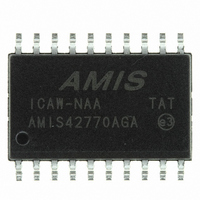
AMIS42770ICAW1RG ON Semiconductor, AMIS42770ICAW1RG Datasheet - Page 6

AMIS42770ICAW1RG
Manufacturer Part Number
AMIS42770ICAW1RG
Description
TRANSCEIVER CAN DUAL HS 20-SOIC
Manufacturer
ON Semiconductor
Type
Transceiverr
Datasheet
1.AMIS42770ICAW1RG.pdf
(13 pages)
Specifications of AMIS42770ICAW1RG
Number Of Drivers/receivers
2/2
Protocol
CAN
Voltage - Supply
4.75 V ~ 5.25 V
Mounting Type
Surface Mount
Package / Case
20-SOIC (7.5mm Width)
Operating Supply Voltage
5.25 V
Supply Current
45 mA
Operating Temperature Range
- 40 C to + 125 C
Mounting Style
SMD/SMT
Product
CAN
Lead Free Status / RoHS Status
Lead free / RoHS Compliant
Other names
766-1010-2
Available stocks
Company
Part Number
Manufacturer
Quantity
Price
Company:
Part Number:
AMIS42770ICAW1RG
Manufacturer:
AD
Quantity:
6 726
Transmitters
line, and a driver control circuit. Each transmitter is
implemented as a push and a pull driver. The drivers will be
active if the transmission of a dominant bit is required. During
the transmission of a recessive bit all drivers are passive. The
transmitters have a built−in current limiting circuit that
protects the driver stages from damage caused by accidental
short circuit to either positive supply voltage or to ground.
Additionally a thermal protection circuit is integrated.
3. Dominant detected by the corresponding receiver.
Receivers
lines. Each receiver section consists of an input filter and a
fast and accurate comparator. The aim of the input filter is
to improve the immunity against high−frequency
disturbances and also to convert the voltage at the bus lines
CANHx and CANLx, which can vary from –12 V to +12 V,
to voltages in the range 0 to 5 V, which can be applied to the
comparators.
signal. In the disabled state (ENBX = high), the output signal
of the comparator will be replaced by a permanently
Table 3. FUNCTION OF THE LOGIC UNIT
The transceiver includes two transmitters, one for each bus
Two bus receiving sections sense the states of the bus
The output signal of the comparators is gated by the ENBx
EN1B
0
0
0
0
0
0
0
0
0
0
0
0
1
1
1
1
1
1
1
1
1
1
1
1
EN2B
0
0
0
0
0
0
1
1
1
1
1
1
0
0
0
0
0
0
1
1
1
1
1
1
TX0
0
0
1
1
1
1
0
0
1
1
1
1
0
0
1
1
1
1
0
0
1
1
1
1
TEXT
0
1
0
1
1
1
0
1
0
1
1
1
0
1
0
1
1
1
0
1
0
1
1
1
(bold letters describe input signals)
dominant (Note 3)
dominant (Note 3)
dominant (Note 3)
dominant (Note 3)
Bus 1 State
dominant
dominant
dominant
recessive
dominant
dominant
dominant
dominant
recessive
recessive
recessive
recessive
recessive
recessive
recessive
recessive
recessive
recessive
recessive
recessive
http://onsemi.com
6
switched on and off with a controlled slope to limit EME.
The driver control circuit will control itself by the thermal
protection circuit, the timer circuit and the logic unit.
switched off by a third device (e.g. the °C). In the disabled
state (ENBx = high) the corresponding transmitter behaves
as in the recessive state.
recessive state and does not depend on the bus voltage. In the
enabled state the receiver signal sent to the logic unit is
identical to the comparator output signal.
Time−out Counter
state on either of the bus lines (blocking all communication),
time−out function is implemented. Signals on pins Tx0 and
Text as well as both bus receivers are connected to the logic
unit through independent timers. If the input of the timer
stays dominant for longer than 25 ms (see parameter t
it is replaced by a recessive signal on the timer output.
The driver control circuit ensures that the drivers are
The enable signal ENBx allows the transmitter to be
To avoid that the transceiver drives a permanent dominant
dominant (Note 3)
dominant (Note 3)
dominant (Note 3)
dominant (Note 3)
Bus 2 State
recessive
recessive
recessive
recessive
recessive
recessive
recessive
recessive
recessive
recessive
recessive
recessive
recessive
dominant
dominant
dominant
dominant
dominant
dominant
dominant
RX0
0
0
0
1
0
0
0
0
0
1
0
1
0
0
0
1
1
0
0
0
0
1
1
1
RINT
0
0
1
1
0
0
0
0
1
1
0
1
0
0
1
1
1
0
0
0
1
1
1
1
dom
),


