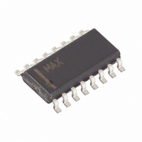
MAX3097ECSE+ Maxim Integrated Products, MAX3097ECSE+ Datasheet - Page 2

MAX3097ECSE+
Manufacturer Part Number
MAX3097ECSE+
Description
IC RCVR TRIPLE RS422/485 16-SOIC
Manufacturer
Maxim Integrated Products
Type
Receiverr
Datasheet
1.MAX3097ECSE.pdf
(16 pages)
Specifications of MAX3097ECSE+
Number Of Drivers/receivers
0/3
Protocol
RS422, RS485
Voltage - Supply
3 V ~ 5.5 V
Mounting Type
Surface Mount
Package / Case
16-SOIC (3.9mm Width)
Data Rate
32 Mbps
Supply Current
3.1 mA
Operating Temperature Range
0 C to + 70 C
Maximum Power Dissipation
696 mW
Mounting Style
SMD/SMT
Lead Free Status / RoHS Status
Lead free / RoHS Compliant
ABSOLUTE MAXIMUM RATINGS
Supply Voltage (V
Receiver Input Voltage (A, A, B, B, Z, Z) .............................±25V
Output Voltage (OUT_, ALARM_)...............-0.3V to (V
DELAY ........................................................-0.3V to (V
Continuous Power Dissipation (T
±15kV ESD-Protected, 32Mbps, 3V/5V,
Triple RS-422/RS-485 Receivers with Fault Detection
Stresses beyond those listed under “Absolute Maximum Ratings” may cause permanent damage to the device. These are stress ratings only, and functional
operation of the device at these or any other conditions beyond those indicated in the operational sections of the specifications is not implied. Exposure to
absolute maximum rating conditions for extended periods may affect device reliability.
ELECTRICAL CHARACTERISTICS
(V
2
Supply Voltage Range
Supply Current
Receiver Differential Threshold
Voltage (Note 1)
Receiver Input Hysteresis
Output High Voltage
Output Low Voltage
Receiver Input Resistance
Input Current
(A , A , B , B (Z , Z )
Output Short-Circuit Current
FAULT DETECTION
MAX3097E Fault-Detection
Receiver Differential Threshold
Voltage (Note 3)
MAX3098EA Fault-Detection
Receiver Differential Threshold
Voltage (Note 3)
16-Pin QSOP (derate 8.3mW/°C above +70°C)............667mW
16-Pin SO (derate 8.7mW/°C above +70°C).................696mW
16-Pin Plastic DIP (derate 10.53mW/°C
CC
above +70°C).............................................................762mW
_______________________________________________________________________________________
= +3V to +5.5V, T
PARAMETER
CC
).............................................................+7V
A
= T
MIN
A
to T
= +70°C)
MAX
SYMBOL
F
F
∆V
F
F
I
V
V
V
V
I
R
OSR
DIFH
DIFL
DIFH
DIFL
I
CC
, unless otherwise noted. Typical values are at V
CC
OH
IN
TH
OL
IN
TH
No load
-10V ≤ V
-10V ≤ V
V
V
V
V
-10V ≤ V
V
0 ≤ V
V
V
CC
CC
CC
CC
CC
CM
CM
CC
CC
= 4.75V, I
= 3.0V, I
= 4.75V, I
= 3.0V, I
= 0 or 5.5V
RO
= 0
= 0
+ 0.3V)
+ 0.3V)
≤ V
CM
CM
CM
CC
≤ 13.2V
≤ 13.2V
≤ 13.2V
O
O
O
O
= -1mA, V
= +1mA, V
CONDITIONS
= -4mA, V
= +4mA, V
Operating Temperature Ranges
Storage Temperature Range .............................-65°C to +150°C
Junction Temperature ......................................................+150°C
Lead Temperature (soldering, 10s) .................................+300°C
MAX3097EC_E...................................................0°C to +70°C
MAX3098E_C_E .................................................0°C to +70°C
MAX3097E_E_E ..............................................-40°C to +85°C
MAX3098E_E_E ..............................................-40°C to +85°C
ID
ID
ID
ID
= 200mV
= -200mV
= 200mV
= -200mV
V
(Note 2)
V
(Note 2)
High limit
Low limit
High limit
Low limit
IN
IN
= 13.2V
= -10V
CC
= +5V and T
V
V
-0.05
-0.20
-200
0.07
-475
0.12
MIN
275
CC
CC
90
3
- 1.5
- 1.0
A
= +25°C.)
TYP
3.1
40
+200
-0.12
MAX
-0.11
±105
-275
0.20
0.14
160
475
5.5
4.0
0.4
0.4
UNITS
mA
mV
mV
mA
mA
mV
kΩ
V
V
V
V


