DS3251+ Maxim Integrated Products, DS3251+ Datasheet - Page 13
DS3251+
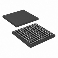
Manufacturer Part Number
DS3251+
Description
IC LIU DS3/E3/STS-1 144-CSBGA
Manufacturer
Maxim Integrated Products
Type
Line Interface Units (LIUs)r
Specifications of DS3251+
Number Of Drivers/receivers
1/1
Protocol
DS3
Voltage - Supply
3.135 V ~ 3.465 V
Mounting Type
Surface Mount
Package / Case
144-CSBGA
Lead Free Status / RoHS Status
Lead free / RoHS Compliant


Table 6-E. Parallel Bus Mode Pin Descriptions
Note: These pins are active in parallel bus mode.
Table 6-F. SPI Bus Mode Pin Descriptions
Note: These pins are active in SPI bus mode.
Note 1:
WR / R/W
RD / DS
RD, WR
NAME
A[5:0]
D[7:0]
NAME
MOT
CPHA
CPOL
SCLK
MOT,
ALE
SDO
INT
CS
ALE
SDI
INT
CS
PIN TYPES
I = input pin
I
O = output pin
O3 = output pin that can be tri-stated
P = power-supply pin
PU
= input pin with internal 10kΩ pullup
TYPE
TYPE
I/O
O
I
I
I
I
I
I
O
O
I
I
I
I
I
I
I
Motorola-Style Parallel CPU Interface
0 = Parallel CPU interface is Intel-style
1 = Parallel CPU interface is Motorola-style
Address Latch Enable. This signal controls a latch on the A[3:0] inputs. For a nonmultiplexed parallel
CPU interface, ALE is wired high to make the latch transparent. For a multiplexed parallel CPU
interface, the falling edge of ALE latches the address.
Chip Select (Active Low). CS must be asserted to read or write internal registers.
Write Enable (Active Low) or Read/Write Select. For the Intel-style parallel CPU interface (MOT =
0), WR is asserted to write internal registers. For the Motorola-style parallel CPU interface (MOT = 1),
R/W determines the type of bus transaction, with R/W = 1 indicating a read and R/W = 0 indicating a
write.
Read Enable (Active Low) or Data Strobe (Active Low). For the Intel-style parallel CPU interface
(MOT = 0), RD is asserted to read internal registers. For the Motorola-style parallel CPU interface
(MOT = 1), the rising edge of DS writes data to internal registers.
Address Bus. These inputs specify the address of the internal register to be accessed. A5 is not
present on the DS3252. A5 and A4 are not present on the DS3251.
Data Bus. These bidirectional lines are inputs during writes to internal registers and outputs during
reads.
Interrupt Output (Active Low, Open Drain). This pin is forced low in response to one or more
unmasked, active interrupt sources within the device. INT remains low until the interrupt is serviced or
masked.
Wire these pins low to enable SPI bus mode.
Wire this pin high when using SPI bus mode.
Chip Select (Active Low). CS must be asserted to read or write internal registers.
Serial Clock for SPI Interface. SCLK is always driven by the SPI bus master.
Serial Data Input for SPI Interface. The SPI bus master transmits data to the device on this pin.
Serial Data Output for SPI Interface
The device transmits data to the SPI bus master on this pin.
SPI Clock Phase
0 = data is latched on the leading edge of the SCLK pulse
1 = data is latched on the trailing edge of the SCLK pulse
SPI Clock Polarity
0 = SCLK is normally low and pulses high during bus transactions
1 = SCLK is normally high and pulses low during bus transactions
Interrupt Output (Active Low, Open Drain). This pin is forced low in response to one or more
unmasked, active interrupt sources within the device. INT remains low until the interrupt is serviced or
masked.
13 of 71
FUNCTION
FUNCTION
Related parts for DS3251+
Image
Part Number
Description
Manufacturer
Datasheet
Request
R

Part Number:
Description:
MAX7528KCWPMaxim Integrated Products [CMOS Dual 8-Bit Buffered Multiplying DACs]
Manufacturer:
Maxim Integrated Products
Datasheet:
Part Number:
Description:
Single +5V, fully integrated, 1.25Gbps laser diode driver.
Manufacturer:
Maxim Integrated Products
Datasheet:
Part Number:
Description:
Single +5V, fully integrated, 155Mbps laser diode driver.
Manufacturer:
Maxim Integrated Products
Datasheet:
Part Number:
Description:
VRD11/VRD10, K8 Rev F 2/3/4-Phase PWM Controllers with Integrated Dual MOSFET Drivers
Manufacturer:
Maxim Integrated Products
Datasheet:
Part Number:
Description:
Highly Integrated Level 2 SMBus Battery Chargers
Manufacturer:
Maxim Integrated Products
Datasheet:
Part Number:
Description:
Current Monitor and Accumulator with Integrated Sense Resistor; ; Temperature Range: -40°C to +85°C
Manufacturer:
Maxim Integrated Products
Part Number:
Description:
TSSOP 14/A�/RS-485 Transceivers with Integrated 100O/120O Termination Resis
Manufacturer:
Maxim Integrated Products
Part Number:
Description:
TSSOP 14/A�/RS-485 Transceivers with Integrated 100O/120O Termination Resis
Manufacturer:
Maxim Integrated Products
Part Number:
Description:
QFN 16/A�/AC-DC and DC-DC Peak-Current-Mode Converters with Integrated Step
Manufacturer:
Maxim Integrated Products
Part Number:
Description:
TDFN/A/65V, 1A, 600KHZ, SYNCHRONOUS STEP-DOWN REGULATOR WITH INTEGRATED SWI
Manufacturer:
Maxim Integrated Products
Part Number:
Description:
Integrated Temperature Controller f
Manufacturer:
Maxim Integrated Products
Part Number:
Description:
SOT23-6/I�/45MHz to 650MHz, Integrated IF VCOs with Differential Output
Manufacturer:
Maxim Integrated Products
Part Number:
Description:
SOT23-6/I�/45MHz to 650MHz, Integrated IF VCOs with Differential Output
Manufacturer:
Maxim Integrated Products
Part Number:
Description:
EVALUATION KIT/2.4GHZ TO 2.5GHZ 802.11G/B RF TRANSCEIVER WITH INTEGRATED PA
Manufacturer:
Maxim Integrated Products
Part Number:
Description:
QFN/E/DUAL PCIE/SATA HIGH SPEED SWITCH WITH INTEGRATED BIAS RESISTOR
Manufacturer:
Maxim Integrated Products
Datasheet: