MAX3089ECSD+ Maxim Integrated Products, MAX3089ECSD+ Datasheet - Page 15
MAX3089ECSD+
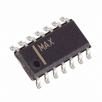
Manufacturer Part Number
MAX3089ECSD+
Description
IC TXRX RS485/422 10MBPS 14-SOIC
Manufacturer
Maxim Integrated Products
Type
Transceiverr
Specifications of MAX3089ECSD+
Number Of Drivers/receivers
1/1
Protocol
RS422, RS485
Voltage - Supply
4.75 V ~ 5.25 V
Mounting Type
Surface Mount
Package / Case
14-SOIC (3.9mm Width), 14-SOL
Package
14SOIC N
Data Transmission Topology
Multidrop|Multipoint
Interface Standards
EIA/TIA-485|RS-422|RS-485
Data Rate
10(Min) Mbps
Function
Cable Transceiver
Number Of Transmitters
1
Transmitter Signal Type
Differential
Transmitter Communication Type
RS-422|RS-485
Driving Mode
3-State
Typical Single Supply Voltage
5 V
Operating Supply Voltage
5 V
Supply Current
0.375 mA
Operating Temperature Range
- 40 C to + 125 C
Input Voltage
5 V
Maximum Power Dissipation
667 mW
Mounting Style
SMD/SMT
Output Current
+/- 1 uA
Output Voltage
+/- 13 V
Product
RS-422/RS-485 Combination
Lead Free Status / RoHS Status
Lead free / RoHS Compliant


±15kV ESD-Protected, Fail-Safe, High-Speed (10Mbps),
Figure 4. MAX3089E Pin Configuration and Functional Diagram
Figure 5. Driver DC Test Load
The ESD-protected pins are tested with reference to the
ground pin in a powered-down condition. They are test-
ed to ±15kV using the Human Body Model.
ESD performance depends on a variety of conditions.
Contact Maxim for a reliability report that documents
test setup, test methodology, and test results.
Figure 14a shows the Human Body Model, and Figure
14b shows the current waveform it generates when dis-
GND
TOP VIEW
SRL
H/F
RO
DE
RE
DI
1
2
3
4
5
6
7
NOTE: SWITCH POSITIONS
INDICATED FOR H/F = GND
Slew-Rate-Limited RS-485/RS-422 Transceivers
MAX3089E
DIP/SO
Y
Z
______________________________________________________________________________________
V
OD
14
13
12
11
10
9
8
V
RXP
A
B
Z
Y
TXP
CC
R
R
RXP
H/F
TXP
ESD Test Conditions
RD
DI
Human Body Model
V
OC
V
CC
RE
GND
charged into a low impedance. This model consists of
a 100pF capacitor charged to the ESD voltage of inter-
est, which is then discharged into the test device
through a 1.5kΩ resistor.
The Machine Model for ESD tests all pins using a
200pF storage capacitor and zero discharge resis-
tance. The objective is to emulate the stress caused
when I/O pins are contacted by handling equipment
during test and assembly. All pins require this protec-
tion, not just RS-485 inputs and outputs.
Figure 6. Receiver Enable/Disable Timing Test Load
DE
MAX3089E
RECEIVER
SRL
OUTPUT
15pF
C
TEST POINT
RL
1k
S1
S2
Machine Model
1k
V
CC
A
B
Z
Y
15
Related parts for MAX3089ECSD+
Image
Part Number
Description
Manufacturer
Datasheet
Request
R

Part Number:
Description:
MAX7528KCWPMaxim Integrated Products [CMOS Dual 8-Bit Buffered Multiplying DACs]
Manufacturer:
Maxim Integrated Products
Datasheet:
Part Number:
Description:
Single +5V, fully integrated, 1.25Gbps laser diode driver.
Manufacturer:
Maxim Integrated Products
Datasheet:
Part Number:
Description:
Single +5V, fully integrated, 155Mbps laser diode driver.
Manufacturer:
Maxim Integrated Products
Datasheet:
Part Number:
Description:
VRD11/VRD10, K8 Rev F 2/3/4-Phase PWM Controllers with Integrated Dual MOSFET Drivers
Manufacturer:
Maxim Integrated Products
Datasheet:
Part Number:
Description:
Highly Integrated Level 2 SMBus Battery Chargers
Manufacturer:
Maxim Integrated Products
Datasheet:
Part Number:
Description:
Current Monitor and Accumulator with Integrated Sense Resistor; ; Temperature Range: -40°C to +85°C
Manufacturer:
Maxim Integrated Products
Part Number:
Description:
TSSOP 14/A�/RS-485 Transceivers with Integrated 100O/120O Termination Resis
Manufacturer:
Maxim Integrated Products
Part Number:
Description:
TSSOP 14/A�/RS-485 Transceivers with Integrated 100O/120O Termination Resis
Manufacturer:
Maxim Integrated Products
Part Number:
Description:
QFN 16/A�/AC-DC and DC-DC Peak-Current-Mode Converters with Integrated Step
Manufacturer:
Maxim Integrated Products
Part Number:
Description:
TDFN/A/65V, 1A, 600KHZ, SYNCHRONOUS STEP-DOWN REGULATOR WITH INTEGRATED SWI
Manufacturer:
Maxim Integrated Products
Part Number:
Description:
Integrated Temperature Controller f
Manufacturer:
Maxim Integrated Products
Part Number:
Description:
SOT23-6/I�/45MHz to 650MHz, Integrated IF VCOs with Differential Output
Manufacturer:
Maxim Integrated Products
Part Number:
Description:
SOT23-6/I�/45MHz to 650MHz, Integrated IF VCOs with Differential Output
Manufacturer:
Maxim Integrated Products
Part Number:
Description:
EVALUATION KIT/2.4GHZ TO 2.5GHZ 802.11G/B RF TRANSCEIVER WITH INTEGRATED PA
Manufacturer:
Maxim Integrated Products
Part Number:
Description:
QFN/E/DUAL PCIE/SATA HIGH SPEED SWITCH WITH INTEGRATED BIAS RESISTOR
Manufacturer:
Maxim Integrated Products
Datasheet: