DS3150QN+ Maxim Integrated Products, DS3150QN+ Datasheet - Page 8
DS3150QN+
Manufacturer Part Number
DS3150QN+
Description
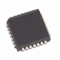
IC LIU T3/E3/STS-1 28-PLCC
Manufacturer
Maxim Integrated Products
Type
Line Interface Units (LIUs)r
Datasheet
1.DS3150T.pdf
(28 pages)
Specifications of DS3150QN+
Number Of Drivers/receivers
1/1
Protocol
DS3
Voltage - Supply
3.135 V ~ 3.465 V
Mounting Type
Surface Mount
Package / Case
28-LCC, 28-PLCC
Lead Free Status / RoHS Status
Lead free / RoHS Compliant


For E3 LOS Assertion:
1) The ALOS circuitry detects that the incoming signal is less than or equal to a signal level
2) The DLOS detector counts 175 ±75 consecutive zeros coming out of the clock and data recovery
For E3 LOS Clear:
1) The ALOS circuitry detects that the incoming signal is greater than or equal to a signal level
2) The DLOS detector counts 175 ±75 consecutive pulse intervals without excessive zero occurrences
The requirements of ANSI T1.231 for STS-1 LOS defects are supported by the DLOS detector. At STS-1
rate, the time required for the DLOS detector to count 175 ±75 consecutive zeros falls in the range of
2.3£T£100ms required by ANSI T1.231 for declaring an LOS defect. Although the time required for the
DLOS detector to count 175 ±75 consecutive pulse intervals with no excessive zeros is less than the
125µs to 250ms period required by ANSI T1.231 for clearing an LOS defect, a period of this length where
LOS is inactive can easily be timed in software.
During LOS, the RCLK output signal is derived from the device’s master clock. The ALOS detector has a
longer time constant than the DLOS detector. Thus, when the incoming signal is lost, the DLOS detector
activates first, asserting the LOS pin, followed by the ALOS detector. When a signal is restored, the
DLOS detector does not get a valid signal that it can qualify for no excessive zero occurrences until the
ALOS detector has seen the incoming signal rise above a signal level approximately 18dB below
nominal.
Framer Interface Format and the B3ZS/HDB3 Decoder. The recovered data can be output in
either NRZ or bipolar format. To select the bipolar format, wire the ZCSE input pin high. In this format,
the B3ZS/HDB3 decoder is disabled, and the recovered data is buffered and output on the RPOS and
RNEG output pins. Received positive-polarity pulses are indicated by RPOS = 1, while negative-polarity
pulses are indicated by RNEG = 1. In bipolar interface format the receiver simply passes on the data
received and does not check it for bipolar violations or excessive zero occurrences.
To select the NRZ format, wire ZCSE low. In this format, the B3ZS/HDB3 decoder is enabled, and the
recovered data is decoded and output as a composite NRZ value on the RNRZ pin. Code violations are
flagged on the RLCV pin. In the discussion that follows, a valid pulse that conforms to the AMI rule is
denoted as B. A pulse that violates the AMI rule is known as bipolar violation (BPV) and is denoted as V.
In DS3 and STS-1 modes, B3ZS decoding is performed. RLCV is asserted during any RCLK cycle where
the data on RNRZ causes ones of the following code violations:
§ A BPV immediately preceded by a valid pulse (B, V)
§ A BPV with the same polarity as the last BPV
approximately 24dB below nominal and mutes the data coming out of the clock and data recovery
block. (24dB below nominal is in the “tolerance range” of G.775, where LOS may or may not be
declared.)
block and asserts LOS. (175 ±75 meets the 10 £ N £ 255 pulse interval duration requirement of
G.775.)
approximately 18dB below nominal and enables data to come out of the clock and data recovery
block. (18dB below nominal is in the “tolerance range” of G.775 where LOS may or may not be
declared.)
and deasserts LOS. (175 ±75 meets the 10 £ N £ 255 pulse interval duration requirement of G.775.)
8 of 28
Related parts for DS3150QN+
Image
Part Number
Description
Manufacturer
Datasheet
Request
R

Part Number:
Description:
3.3V T3 / E3 / STS-1 Line Interface Unit
Manufacturer:
Maxim Integrated Products
Datasheet:
Part Number:
Description:
MAX7528KCWPMaxim Integrated Products [CMOS Dual 8-Bit Buffered Multiplying DACs]
Manufacturer:
Maxim Integrated Products
Datasheet:
Part Number:
Description:
Single +5V, fully integrated, 1.25Gbps laser diode driver.
Manufacturer:
Maxim Integrated Products
Datasheet:
Part Number:
Description:
Single +5V, fully integrated, 155Mbps laser diode driver.
Manufacturer:
Maxim Integrated Products
Datasheet:
Part Number:
Description:
VRD11/VRD10, K8 Rev F 2/3/4-Phase PWM Controllers with Integrated Dual MOSFET Drivers
Manufacturer:
Maxim Integrated Products
Datasheet:
Part Number:
Description:
Highly Integrated Level 2 SMBus Battery Chargers
Manufacturer:
Maxim Integrated Products
Datasheet:
Part Number:
Description:
Current Monitor and Accumulator with Integrated Sense Resistor; ; Temperature Range: -40°C to +85°C
Manufacturer:
Maxim Integrated Products
Part Number:
Description:
TSSOP 14/A�/RS-485 Transceivers with Integrated 100O/120O Termination Resis
Manufacturer:
Maxim Integrated Products
Part Number:
Description:
TSSOP 14/A�/RS-485 Transceivers with Integrated 100O/120O Termination Resis
Manufacturer:
Maxim Integrated Products
Part Number:
Description:
QFN 16/A�/AC-DC and DC-DC Peak-Current-Mode Converters with Integrated Step
Manufacturer:
Maxim Integrated Products
Part Number:
Description:
TDFN/A/65V, 1A, 600KHZ, SYNCHRONOUS STEP-DOWN REGULATOR WITH INTEGRATED SWI
Manufacturer:
Maxim Integrated Products
Part Number:
Description:
Integrated Temperature Controller f
Manufacturer:
Maxim Integrated Products
Part Number:
Description:
SOT23-6/I�/45MHz to 650MHz, Integrated IF VCOs with Differential Output
Manufacturer:
Maxim Integrated Products
Part Number:
Description:
SOT23-6/I�/45MHz to 650MHz, Integrated IF VCOs with Differential Output
Manufacturer:
Maxim Integrated Products
Part Number:
Description:
EVALUATION KIT/2.4GHZ TO 2.5GHZ 802.11G/B RF TRANSCEIVER WITH INTEGRATED PA
Manufacturer:
Maxim Integrated Products