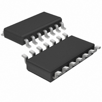
LTC491IS#TR Linear Technology, LTC491IS#TR Datasheet - Page 2

LTC491IS#TR
Manufacturer Part Number
LTC491IS#TR
Description
IC TXRX RS485 LOW POWER 14-SOIC
Manufacturer
Linear Technology
Type
Transceiverr
Datasheet
1.LTC491CNPBF.pdf
(12 pages)
Specifications of LTC491IS#TR
Number Of Drivers/receivers
1/1
Protocol
RS422, RS485
Voltage - Supply
4.75 V ~ 5.25 V
Mounting Type
Surface Mount
Package / Case
14-SOIC (3.9mm Width), 14-SOL
Lead Free Status / RoHS Status
Contains lead / RoHS non-compliant
Available stocks
Company
Part Number
Manufacturer
Quantity
Price
DC ELECTRICAL CHARACTERISTICS
A
SYMBOL
V
V
V
V
V
l
l
V
V
V
I
I
R
I
I
I
I
(Note 1)
Supply Voltage (V
Control Input Voltages .................... –0.5V to V
Control Input Currents .......................... –50mA to 50mA
Driver Input Voltages ...................... –0.5V to V
Driver Input Currents ............................ –25mA to 25mA
Driver Output Voltages .......................................... 14V
Receiver Input Voltages ......................................... 14V
Receiver Output Voltages ............... –0.5V to V
Operating Temperature Range
Storage Temperature Range ................. – 65 C to 150 C
Lead Temperature (Soldering, 10 sec).................. 300 C
temperature range, otherwise specifications are at T
LTC491
2
IN1
IN2
OZR
CC
OSD1
OSD2
OSR
OZ
OD1
OD2
OC
IH
IL
TH
OH
OL
V
V
IN
BSOLUTE
OD
TH
LTC491C ................................................. 0 C to 70 C
LTC491I .............................................. – 40 C to 85 C
V
OC
PARAMETER
Differential Driver Output Voltage (Unloaded)
Differential Driver Output Voltage (With load)
Change in Magnitude of Driver Differential Output
Voltage for Complementary Output States
Driver Common Mode Output Voltage
Change in Magnitude of Driver Common Mode
Output Voltage for Complementary Output States
Input High Voltage
Input Low Voltage
Input Current
Input Current (A, B)
Differential Input Threshold Voltage for Receiver
Receiver Input Hysteresis
Receiver Output High Voltage
Receiver Output Low Voltage
Three-State Output Current at Receiver
Supply Current
Receiver Input Resistance
Driver Short Circuit Current, V
Driver Short Circuit Current, V
Receiver Short Circuit Current
Driver Three-State Output Current
CC
W
) ............................................... 12V
A
XI
W
U
OUT
OUT
W
= High
= Low
R
A
TI
U
A
CC
CC
CC
= 25 C. V
G
+ 0.5V
+ 0.5V
+ 0.5V
S
CONDITIONS
I
R = 50 ; (RS422)
R = 27 ; (RS485) (Figure 1)
R = 27 or R = 50 (Figure 1)
D, DE, REB
V
– 7V V
V
I
I
V
No Load; D = GND,
or V
– 7V V
V
V
0V V
V
O
O
O
CC
CM
CC
O
O
O
= 0
= –4mA, V
= 4mA, V
= – 7V
= 12V
= – 7V to 12V
CC
= 0V or 5.25V
= Max 0.4V V
CC
= 0V
The
O
= 5V 5%
CM
CM
V
PACKAGE/ORDER I FOR ATIO
Consult LTC Marketing for parts specified with wider operating temperature ranges.
CC
ID
12V
denotes the specifications which apply over the full operating
12V
ID
= –0.2V
14-LEAD PDIP
= 0.2V
GND
GND
N PACKAGE
REB
NC
DE
T
T
R
D
JMAX
JMAX
O
V
Outputs Disabled
1
2
3
4
5
6
7
V
Outputs Enabled
2.4V
IN
= 100 C,
= 100 C,
IN
= 12V
= –7V
TOP VIEW
R
D
JA
JA
14-LEAD PLASTIC SO
= 90 C/W (N)
= 110 C/W (S)
S PACKAGE
14
13
12
11
10
9
8
Y
V
NC
A
B
Z
NC
CC
– 0.2
MIN
1.5
2.0
3.5
12
2
7
U
TYP
300
300
100
100
70
ORDER PART
2
LTC491CN
LTC491CS
LTC491IN
LTC491IS
NUMBER
W
MAX
– 0.8
500
500
250
250
0.2
0.2
0.8
1.0
0.4
0.2
85
200
5
5
3
2
1
UNITS
U
491fa
mA
mA
mV
mA
mA
mA
k
V
V
V
V
V
V
V
V
A
V
V
V
A
A
A
A


