ATA6831-PIQW Atmel, ATA6831-PIQW Datasheet
ATA6831-PIQW
Specifications of ATA6831-PIQW


Related parts for ATA6831-PIQW


ATA6831-PIQW Summary of contents
Page 1
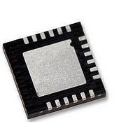
... QFN18 Package 1. Description ® The Atmel ATA6831 provides fully protected driver interfaces designed in SOI tech- nology. They are used to allow a microcontroller to control up to three different loads in automotive and industrial applications. Each of the three high-side and three low-side drivers is capable of driving currents ...
Page 2
... Figure 1-1. Block Diagram Input register Ouput register CLK Fault DO detector 7 PWM 6 Fault detector 1 OUT3S Atmel ATA6831 Serial interface Fault Fault detector detector Fault Fault detector detector OUT3F OUT2S OUT2F OUT1S Charge pump protection Control logic Power on reset Thermal protection 15 OUT1F ...
Page 3
... OUT1S Used only for final testing connected to OUT1F 17 PGND1 Power ground OUT1 18 PGND3 Power ground OUT3 4908I–AUTO–01/ OUT3S 1 12 OUT2F OUT3F 2 11 VS2 VS1 DI 4 VCC 9 CLK 5 8 GND PWM Atmel ATA6831 = 2MHz) max 3 ...
Page 4
... CLK DO TP S1L S1H Table 3-1. Bit Atmel ATA6831 4 LS2 HS2 LS3 HS3 PL1 PH1 S2L S2H S3L S3H Input Data Protocol Input Register Function Status register reset (high = reset; the bits PSF and OVL in the output SRR data register are set to low) ...
Page 5
... High = standby, low = normal operation PSF Power-supply fail: undervoltage at pin VS detected Bit 10 Bit 9 Bit 8 Bit 7 PH2 PL2 PH1 PL1 Bit 10 Bit 9 Bit 8 Bit Atmel ATA6831 Bit 6 Bit 5 Bit 4 Bit 3 Bit 2 HS3 LS3 HS2 LS2 HS1 Bit 6 Bit 5 Bit 4 Bit 3 Bit 2 (HS3) (LS3) (HS2) (LS2) (HS1 ...
Page 6
... I /I Out1-3L Switching on an output stage with the OLD bit set to low disables the open-load function for this output. Figure 3-2. Atmel ATA6831 6 . The outputs are enabled immediately when the supply dUV Figure 3-2. . ...
Page 7
... Inhibit The SI bit in the input register has to be set to zero to inhibit the Atmel ATA6831. In this state, all output stages are then turned off but the serial interface remains active. The current consumption is reduced to less than 2µA at pin VS and less than 100µA at pin VCC. The output stages can be reactivated by setting bit SI to “ ...
Page 8
... Thermal resistance from junction to case Thermal resistance from junction to ambient 6. Operating Range Parameters Supply voltage Logic supply voltage Logic input voltage Serial interface clock frequency PWM input frequency Junction temperature range Note: 1. Threshold for undervoltage description Atmel ATA6831 8 Pin Symbol 10 10 VCC V ...
Page 9
... I VCC = 32.5V, INH = low 10 40V, INH = low 10 VCC dPor = dUV T jPW set T jPW reset switch off T j switch on Atmel ATA6831 Value (1) Level 4 Level 5 2kV 500V Min. Typ. Max 100 350 650 0.5 5 3.2 3.9 4.4 VCC 30 95 190 5 ...
Page 10
... Delay time between rising/falling edge of input signal at pin PWM and switch on/off output stages to 90% of final level. 3. Difference between switch-on and switch-off delay time of input signal at pin PWM to output stages in PWM mode. Atmel ATA6831 10 < 150°C; unless otherwise specified, all values refer to GND pins. ...
Page 11
... CLK, PWM VCC = 0V 3 Atmel ATA6831 Min. Typ. Max. –6 –9 –11 0.5 1.5 2 Out1- don t 20 don t 20 doff t 3 doff – doff = 20 – t doff = -5 5 – t doff 0 ...
Page 12
... CLK period time 8.12 CLK setup time 8.13 CLK setup time 8.14 DI setup time 8.15 DI hold time *) Type means: A =100% tested 100% correlation tested Characterized on samples Design parameter Atmel ATA6831 12 < 150°C; unless otherwise specified, all values refer to GND pins. j Symbol Pin ...
Page 13
... Figure 9-1. Serial Interface Timing with Chart Number CS 4 CLK 3 DI CLK DO Inputs DI, CLK, CS: High level = 0.7 Output DO: High level = 0.8 4908I–AUTO–01/ low level = 0 low level = 0 Atmel ATA6831 ...
Page 14
... Electrolytic capacitor C > 22µF in parallel with a ceramic capacitor C = 100nF. The • Recommended value for capacitors at V – Electrolytic capacitor C > 10µF in parallel with a ceramic capacitor C = 100nF. • To reduce thermal resistance, place cooling areas on the PCB as close as possible to the GND pins and to the die pad. Atmel ATA6831 ...
Page 15
... Ordering Information Extended Type Number ATA6831-PIQW 12. Package Information Package: VQFN_4 x 4_18L Exposed pad 2.7 x 3.175 Dimensions in mm Not indicated tolerances ±0.05 Pin 1 identification Drawing-No.: 6.543-5133.01-4 Issue: 1; 26.04.07 4908I–AUTO–01/11 Package Remarks QFN18, 4mm 4mm Taped and reeled, Pb-free Top 0.2 0.9 ± ...
Page 16
... Revision No. 4908I-AUTO-01/11 4908H-AUTO-10/10 4908G-AUTO-07/10 4908F-AUTO-02/10 4908E-AUTO-06/07 4908D-AUTO-09/06 4908C-AUTO-08/06 Atmel ATA6831 16 History Features on page 1 changed Section 3.6 “Inhibit” on page 7 changed Section 8 “Electrical Characteristics” number 1.1 on page 9 changed Ordering Information table on page 15 changed Section 3.3 Open-load Detection on page 6 changed Section 8 “Electrical Characteristics” numbers 4.12 and 4.13 on pages changed Section 8 “ ...
Page 17
... Disclaimer: The information in this document is provided in connection with Atmel products. No license, express or implied, by estoppel or otherwise, to any intellec- tual property right is granted by this document or in connection with the sale of Atmel products. EXCEPT AS SET FORTH IN THE ATMEL TERMS AND CONDITIONS OF SALES LOCATED ON THE ATMEL WEBSITE, ATMEL ASSUMES NO LIABILITY WHATSOEVER AND DISCLAIMS ANY EXPRESS, IMPLIED OR STATUTORY WARRANTY RELATING TO ITS PRODUCTS INCLUDING, BUT NOT LIMITED TO, THE IMPLIED WARRANTY OF MERCHANTABILITY, FITNESS FOR A PARTICU- LAR PURPOSE, OR NON-INFRINGEMENT ...