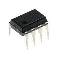
NCP1055P100 ON Semiconductor, NCP1055P100 Datasheet - Page 15

NCP1055P100
Manufacturer Part Number
NCP1055P100
Description
Other Power Management 700V 680mA Switching
Manufacturer
ON Semiconductor
Type
Monolithic High Voltage Regulatorsr
Datasheet
1.NCP1053P136.pdf
(25 pages)
Specifications of NCP1055P100
Input Voltage Range
- 0.3 V to + 10 V
Operating Temperature Range
- 40 C to + 150 C
Mounting Style
Through Hole
Package / Case
PDIP-8
Lead Free Status / Rohs Status
Lead free / RoHS Compliant
Current Limit Comparator and Power Switch Circuit
SENSEFET™ in order to monitor the drain current. A
portion of the current flowing through the circuit goes into
a sense element, R
if the voltage across R
is present at its inverting input. If this level is exceeded, the
comparator quickly resets the Turn Off Latch, thus
protecting the Power Switch Circuit.
sensing signal path to prevent a premature reset of the Turn
Off Latch. A potential premature reset signal is generated
each time the Power Switch Circuit is driven into conduction
and appears as a narrow voltage spike across current sense
resistor R
gate to source capacitance, transformer interwinding
capacitance, and output rectifier recovery time. The Leading
Edge Blanking circuit has a dynamic behavior that masks the
current signal until the Power Switch Circuit turn−on
transition is completed. The current limit propagation delay
time is typically 135 to 165 nanoseconds. This time is
measured from when an overcurrent appears at the Power
Switch Circuit drain, to the beginning of turn−off. Care must
be taken during transformer saturation so that the maximum
device current limit rating is not exceeded.
integrated with the control logic circuitry and is designed to
directly drive the converter transformer. Because the
characteristics of the power switch circuit are well known,
the gate drive has been tailored to control switching
transitions to help limit electromagnetic interference (EMI).
The Power Switch Circuit is capable of switching 700 V
with an associated drain current that ranges nominally from
0.10 to 0.68 Amps.
Startup Circuit
on Pin 5, through the primary winding. The circuit is
self−biasing and acts as a constant current source, gated by
control logic. Upon application of the AC line voltage, this
circuit routes current into the supply capacitor typically
connected to Pin 1. During normal operation, this capacitor
is hysteretically regulated from 7.5 to 8.5 V by monitoring
the supply voltage with a comparator and controlling the
startup current source accordingly. This Dynamic
Self−Supply (DSS) functionality offers a great deal of
applications flexibility as well. The startup circuit is rated at
a maximum 700 V (maximum power dissipation limits must
be observed).
The Power Switch Circuit is constructed with a
A Leading Edge Blanking circuit was placed in the current
The high voltage Power Switch Circuit is monolithically
Rectified AC line voltage is applied to the Startup Circuit
sense
. The spike is due to the Power Switch Circuit
sense
. The current limit comparator detects
sense
exceeds the reference level that
http://onsemi.com
15
Undervoltage Lockout
included to guarantee that the integrated circuit has
sufficient voltage to be fully functional. The UVLO
comparator monitors the supply capacitor input voltage at
Pin 1 and disables the Power Switch Circuit whenever the
capacitor voltage drops below the undervoltage lockout
threshold. When this level is crossed, the controller enters a
new startup phase by turning the current source on. The
supply voltage will then have to exceed the startup threshold
in order to turn off the startup current source. Startup and
normal operation of the converter are shown in Figure 3.
Fault Detector
circuitry for detecting application fault conditions such as
open loop, overload or a short circuited output. A timer is
generated by driving the supply capacitor with a known
current and hysteretically regulating the supply voltage
between set thresholds. The timer period starts when the
supply voltage reaches the nominal upper threshold of 8.5 V
and stops when the drain current of the integrated circuit
draws the supply capacitor voltage down to the undervoltage
lockout threshold of 7.5 V.
to the control input, the fault detect logic is set to indicate an
abnormal condition. This may occur, for example, when the
optocoupler fails or the output of the application is
overloaded or completely shorted. In this case, the part will
stop switching, go into a low power mode, and begin to draw
down the supply capacitor to the reset threshold voltage of
4.5 V. At that time, the startup circuit will turn on again to
drive the supply to the turn on threshold. Then the part will
begin the cycle again, effectively sampling the control input
to determine if the fault condition has been removed. This
mode is commonly referred to as burst mode operation and
is shown is Figure 4.
startup with monotonically increasing output voltage,
without falsely sensing a fault condition. Figure 4 shows
successful startup and the evolution of the signals involved
in the presence of a fault.
Thermal Shutdown
in the event that the maximum junction temperature is
exceeded. When activated, typically at 160°C, one input of
the Driver is held low to disable the Power Switch Circuit.
The Power Switch is allowed to resume operation when the
junction temperature falls below 85°C. The thermal
shutdown feature is provided to prevent catastrophic device
failures from accidental overheating. It is not intended to be
used as a substitute for proper heatsinking.
An Undervoltage Lockout (UVLO) comparator is
The NCP105X series has integrated Fault Detector
If, during this timer period, no feedback has been applied
Proper selection of the supply capacitor allows successful
The internal Thermal Shutdown block protects the device


