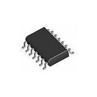
HV9110NG Supertex, HV9110NG Datasheet - Page 5

HV9110NG
Manufacturer Part Number
HV9110NG
Description
Switching Converters, Regulators & Controllers HVCMOS
Manufacturer
Supertex
Datasheet
1.HV9110NG-G.pdf
(8 pages)
Specifications of HV9110NG
Output Voltage
4.08 V
Mounting Style
SMD/SMT
Package / Case
SOIC-14
Lead Free Status / Rohs Status
Lead free / RoHS Compliant
Available stocks
Company
Part Number
Manufacturer
Quantity
Price
Part Number:
HV9110NG(S267)
Manufacturer:
SUPERTEX
Quantity:
20 000
Test Circuits
Detailed Description
Preregulator
The preregulator/startup circuit for the HV9110 consists of a
high-voltage, n-channel, depletion-mode, DMOS transistor
driven by an error amplifier to form a variable current path
between the VIN terminal and the VDD terminal. The maxi-
mum current (about 20mA) occurs when V
reducing as V
V
is held at 10 or 12V by an external source (generally the
supply the chip is controlling), no current other than leakage
is drawn through the high voltage transistor. This minimizes
dissipation.
An external capacitor between VDD and VSS is generally
required to store energy used by the chip in the time be-
tween shutoff of the high voltage path and the VDD supply’s
output rising enough to take over powering the chip. This
capacitor should have a value of 100X or more the effective
gate capacitance of the MOSFET being driven, i.e.,
C
as well as very good high frequency characteristics. Stacked
polyester or ceramic caps work well. Electrolytic capacitors
are generally not suitable.
A common resistor divider string is used to monitor V
both the under voltage lockout circuit and the shutoff circuit
of the high voltage FET. Setting the under voltage sense
point about 0.6V lower on the string than the FET shutoff
point guarantees that the under voltage lockout always re-
leases before the FET shuts off.
DD
STORAGE
rises to somewhere between 7.8 and 9.4V, so that if V
+10V
(V
(–V
GND
DD
NOTE:
(FB)
IN
)
≥ 100 x (gate charge of FET at 10V)
Set Feedback Voltage so that V
)
Reference
DD
connecting transformer
rises. This path shuts off altogether when
0.1µF
Error Amp Z
+
–
1.0V swept 100Hz – 2.2MHz
●
COMP
V
1
1235 Bordeaux Drive, Sunnyvale, CA 94089
OUT
= V
secondary)
Tektronix
P6021
(1 turn
DIVIDE
DD
= 0, with current
± 1.0mV before
V
2
60.4K
40.2K
DD
for
DD
5
Bias Circuit
An external bias resistor, connected between the BIAS pin
and VSS is required by the HV9110 to set currents in a se-
ries of current mirrors used by the analog sections of the
chip. The nominal external bias current requirement is 15 to
20µA, which can be set by a 390KΩ to 510KΩ resistor if a
10V V
12V. A precision resistor is not required; ± 5% is fine.
Clock Oscillator
The clock oscillator of the HV9110 consists of a ring of
CMOS inverters, timing capacitors, and a frequency dividing
flip-flop. A single external resistor between the OSC IN and
OSC OUT is required to set the oscillator frequency (see
graph). One major difference exists between the Supertex
HV9110 and competitive 9110s. On the Supertex part, the
oscillator is shut off when a shutoff command is received.
This saves about 150µA of quiescent current, which aids in
the construction of power supplies that meet CCITT specifi-
cation I-430, and in other situations where an absolute mini-
mum of quiescent power dissipation is required.
0.1V swept 10Hz – 1MHz
DD
is used, or a 510kΩ to 680KΩ resistor if V
10.0V
●
Tel: 408-222-8888
4.00V
Reference
100K1%
0.1µF
PSRR
●
www.supertex.com
+
–
100K1%
V
2
V
HV9110
1
DD
will be


