MC1413BDG ON Semiconductor, MC1413BDG Datasheet

IC TRANS ARRAY DARL HV 16SOIC

MC1413BDG

Manufacturer Part Number
MC1413BDG
Description
IC TRANS ARRAY DARL HV 16SOIC
Manufacturer
ON Semiconductor
Type
Darlington Arrayr
Datasheet

Specifications of MC1413BDG

Number Of Drivers/receivers
7/0
Voltage - Supply
5V
Mounting Type
Surface Mount
Package / Case
16-SOIC (3.9mm Width)
Configuration
Array 7
Transistor Polarity
NPN
Mounting Style
SMD/SMT
Collector- Emitter Voltage Vceo Max
50 V
Maximum Dc Collector Current
0.5 A
Maximum Operating Temperature
+ 85 C
Dc Collector/base Gain Hfe Min
1000
Minimum Operating Temperature
- 40 C
Module Configuration
Seven
Collector Emitter Voltage V(br)ceo
50V
Dc Collector Current
500mA
Dc Current Gain Hfe
1000
Rohs Compliant
Yes
Lead Free Status / RoHS Status
Lead free / RoHS Compliant
Protocol
-
Lead Free Status / Rohs Status
Lead free / RoHS Compliant
Other names
MC1413BDGOS

Available stocks

Company
Part Number
Manufacturer
Quantity
Price
Part Number:
MC1413BDG
Manufacturer:
ON
Quantity:
15 000
Part Number:
MC1413BDG
Manufacturer:
ON
Quantity:
80
Part Number:
MC1413BDG
Manufacturer:
ON/安森美
Quantity:
20 000
MC1413, MC1413B,
NCV1413B
High Voltage, High Current
Darlington Transistor Arrays
well suited for driving lamps, relays, or printer hammers in a variety of
industrial and consumer applications. Their high breakdown voltage
and internal suppression diodes insure freedom from problems
associated with inductive loads. Peak inrush currents to 500 mA
permit them to drive incandescent lamps.
systems utilizing a 5.0 V TTL or CMOS Logic.
Features
*For additional information on our Pb−Free strategy and soldering details, please
© Semiconductor Components Industries, LLC, 2006
July, 2006 − Rev. 8
download the ON Semiconductor Soldering and Mounting Techniques Reference
Manual, SOLDERRM/D.
The seven NPN Darlington connected transistors in these arrays are
The MC1413, B with a 2.7 kW series input resistor is well suited for
and Control Changes
Pb−Free Packages are Available*
NCV Prefix for Automotive and Other Applications Requiring Site
Figure 1. Representative Schematic Diagram
Figure 2. PIN CONNECTIONS
1
2
3
4
5
6
7
8
2.7 k
5.0 k
(Top View)
1/7 MC1413, B
3.0 k
16
15
14
13
10
12
11
9
Pin 9
1
MC1413D
MC1413DG
MC1413DR2
MC1413DR2G
MC1413P
MC1413PG
MC1413BD
MC1413BDG
MC1413BDR2
MC1413BDR2G
MC1413BP
MC1413BPG
NCV1413BDR2
NCV1413BDR2G
†For information on tape and reel specifications,
See general marking information in the device marking
section on page 5 of this data sheet.
including part orientation and tape sizes, please
refer to our Tape and Reel Packaging Specifications
Brochure, BRD8011/D.
Device
DEVICE MARKING INFORMATION
16
16
1
ORDERING INFORMATION
http://onsemi.com
1
(Pb−Free)
(Pb−Free)
(Pb−Free)
(Pb−Free)
(Pb−Free)
(Pb−Free)
(Pb−Free)
SOIC−16
SOIC−16
SOIC−16
SOIC−16
SOIC−16
SOIC−16
SOIC−16
SOIC−16
SOIC−16
SOIC−16
Package
PDIP−16
PDIP−16
PDIP−16
PDIP−16
Publication Order Number:
2500 Tape & Reel
2500 Tape & Reel
2500 Tape & Reel
2500 Tape & Reel
2500 Tape & Reel
2500 Tape & Reel
CASE 751B
CASE 648
P SUFFIX
D SUFFIX
PDIP−16
SOIC−16
48 Units/Tube
48 Units/Rail
25 Units/Rail
25 Units/Rail
48 Units/Rail
48 Units/Rail
25 Units/Rail
25 Units/Rail
Shipping
MC1413/D

Related parts for MC1413BDG

MC1413BDG Summary of contents

Page 1

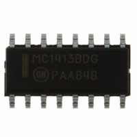
... ON Semiconductor Soldering and Mounting Techniques Reference Manual, SOLDERRM/D. © Semiconductor Components Industries, LLC, 2006 July, 2006 − Rev. 8 Pin 9 MC1413D MC1413DG MC1413DR2 MC1413DR2G MC1413P MC1413PG 16 MC1413BD MC1413BDG 15 MC1413BDR2 14 MC1413BDR2G 13 MC1413BP MC1413BPG 12 NCV1413BDR2 11 NCV1413BDR2G 10 †For information on tape and reel specifications, ...

Page 2

MAXIMUM RATINGS (T = 25°C, and rating apply to any one device in the package, unless otherwise noted.) A Output Voltage Input Voltage Collector Current − Continuous Base Current − Continuous Operating Ambient Temperature Range MC1413 MC1413B NCV1413B Storage Temperature ...

Page 3

ELECTRICAL CHARACTERISTICS Characteristic Output Leakage Current ( +85° +25° Collector−Emitter Saturation Voltage = 500 mA 350 mA 350 mA) ...

Page 4

TYPICAL PERFORMANCE CURVES − T 400 300 MC1413, B 200 100 0 0 1.0 2.0 3.0 4.0 5.0 8 INPUT VOLTAGE (V) I Figure 3. Output Current versus Input Voltage 800 700 600 PIN 10 1 Output Conducting ...

Page 5

... MC1413, MC1413B, NCV1413B MARKING DIAGRAMS PDIP−16 P SUFFIX CASE 648 16 MC1413P ULN2003A AWLYYWWG 1 SOIC−16 D SUFFIX CASE 751B 16 16 MC1413DG MC1413BDG AWLYWW AWLYWW Assembly Location WL = Wafer Lot YY Year WW = Work Week G = Pb−Free Package http://onsemi.com 5 16 MC1413BP ULQ2003A AWLYYWWG 1 16 NCV1413BDG ...

Page 6

MC1413, MC1413B, NCV1413B −A− −T− 0.25 (0.010 PACKAGE DIMENSIONS PDIP−16 P SUFFIX CASE 648−08 ISSUE T NOTES: 1. DIMENSIONING AND TOLERANCING PER 2. CONTROLLING ...

Page 7

G K −T− SEATING PLANE 0.25 (0.010 MC1413, MC1413B, NCV1413B PACKAGE DIMENSIONS SOIC−16 D SUFFIX CASE 751B−05 ISSUE J −B− 0.25 (0.010 ...

Page 8

... Opportunity/Affirmative Action Employer. This literature is subject to all applicable copyright laws and is not for resale in any manner. PUBLICATION ORDERING INFORMATION LITERATURE FULFILLMENT: Literature Distribution Center for ON Semiconductor P.O. Box 5163, Denver, Colorado 80217 USA Phone: 303−675−2175 or 800−344−3860 Toll Free USA/Canada Fax: 303− ...

Related keywords