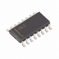
MAX202CSE+T Maxim Integrated Products, MAX202CSE+T Datasheet - Page 5

MAX202CSE+T
Manufacturer Part Number
MAX202CSE+T
Description
IC TXRX RS-232 W/CAP 16-SOIC
Manufacturer
Maxim Integrated Products
Type
Transceiverr
Datasheet
1.MAX202CPE.pdf
(23 pages)
Specifications of MAX202CSE+T
Number Of Drivers/receivers
2/2
Protocol
RS232
Voltage - Supply
4.5 V ~ 5.5 V
Mounting Type
Surface Mount
Package / Case
16-SOIC (3.9mm Width)
Lead Free Status / RoHS Status
Lead free / RoHS Compliant
Figure 1. Shutdown Current Test Circuit
Figure 2. Receiver Output Enable and Disable Timing
0V OR +5.5V
DRIVE
+5.5V
+5.5V (0)
0.1FF
0.1FF
0.1FF
+5.5V
RECEIVER
OUTPUTS
NOTE: POLARITY OF EN IS REVERSED FOR THE MAX213.
INPUT
RECEIVER
OUTPUT
C
INPUT
L
= 150pF
EN
EN
NOTE 1: ( ) ARE FOR MAX213.
NOTE 2: CAPACITORS CAN BE POLARIZED OR UNPOLARIZED.
C1+
C1-
C2+
C2-
T
R
EN (EN)
SHDN
(SHDN)
+3V
IN
OUT
0V
400kI
V
V
OH
OL
I
SHDN
0V
+5.5V
+3V
R1 T0 R5
+3.5V
+0.8V
V
V
MAX200
MAX205
MAX206
MAX211
MAX213
OUTPUT ENABLE TIME
OL
OH
R
GND
V
OUTPUT ENABLE TIME
+ 0.1V
L
- 0.1V
CC
= 1kI
T1 T0 T5
+ 2.5V
0.1FF
with 0.1µF External Capacitors
5kI
T
OUT
R
V+
V-
IN
+5.5V
3kI
0.1FF
+5V, RS-232 Transceivers
The MAX200–MAX209/MAX211/MAX213 consist of
three sections: charge-pump voltage converters, drivers
(transmitters), and receivers. Each section is described
in detail.
The +5V to Q10V conversion is performed by two
charge-pump voltage converters (Figure 4). The first
uses capacitor C1 to double +5V to +10V, storing +10V
on the V+ output filter capacitor, C3. The second charge-
pump voltage converter uses capacitor C2 to invert +10V
to -10V, storing -10V on the V- output filter capacitor, C4.
The MAX201 and MAX209 include only the V+ to V-
charge pump, and are intended for applications that
have a V
+13.2V range.
In shutdown mode, V+ is internally connected to V
a 1kI pulldown resistor and V- is internally connected to
ground by a 1kI pullup resistor.
When V
is Q8V when loaded with a nominal 5kI RS-232 receiver.
The output swing is guaranteed to meet the EIA/TIA-232E
and V.28 specifications, which call for Q5V minimum out-
put levels under worst-case conditions. These include
a minimum 3kI load, V
operating temperature. The open-circuit output-voltage
swing ranges from (V+ - 0.6V) to V-.
Input thresholds are both CMOS and TTL compatible.
The inputs of unused drivers can be left unconnected
since 400kI pullup resistors to V
chip. Since all drivers invert, the pullup resistors force
the outputs of unused drivers low. The input pullup resis-
tors typically source 15µA; therefore, the driver inputs
should be driven high or open circuited to minimize
power-supply current in shutdown mode.
When in low-power shutdown mode, the driver outputs
are turned off and their leakage current is less than 1mA,
even if the transmitter output is backdriven between 0V
and (V
diode clamped to ground with a 1kI series impedance.
The transmitter output is also zener clamped to approxi-
mately (V
CC
CC
CC
CC
+ 6V). Below -0.5V, the transmitter output is
= +5V, the typical driver output-voltage swing
= +5V supply and a V+ supply in the +9V to
+ 6V), with a 1kI series impedance.
+5V to ± 10V Dual Charge-Pump
Detailed Description
CC
= +4.5V, and the maximum
Voltage Converter
CC
RS-232 Drivers
are included on-
CC
by
5


