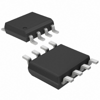
MAX13085EASA+T Maxim Integrated Products, MAX13085EASA+T Datasheet - Page 15

MAX13085EASA+T
Manufacturer Part Number
MAX13085EASA+T
Description
IC TXRX RS485/RS422 8-SOIC
Manufacturer
Maxim Integrated Products
Type
Transceiverr
Datasheet
1.MAX13082ECSA.pdf
(24 pages)
Specifications of MAX13085EASA+T
Number Of Drivers/receivers
1/1
Protocol
RS422, RS485
Voltage - Supply
4.5 V ~ 5.5 V
Mounting Type
Surface Mount
Package / Case
8-SOIC (3.9mm Width)
Lead Free Status / RoHS Status
Lead free / RoHS Compliant
The MAX13080E–MAX13089E high-speed transceivers
for RS-485/RS-422 communication contain one driver
and one receiver. These devices feature fail-safe circuit-
ry, which guarantees a logic-high receiver output when
the receiver inputs are open or shorted, or when they are
connected to a terminated transmission line with all dri-
vers disabled (see the Fail-Safe section). The
MAX13080E/MAX13082E/MAX13083E/MAX13085E/
MAX13086E/MAX13088E/MAX13089E also feature a hot-
swap capability allowing line insertion without erroneous
data transfer (see the Hot Swap Capability section). The
MAX13080E/MAX13081E/MAX13082E feature reduced
slew-rate drivers that minimize EMI and reduce reflec-
tions caused by improperly terminated cables, allowing
error-free data transmission up to 250kbps. The
MAX13083E/MAX13084E/MAX13085E also offer slew-
rate limits allowing transmit speeds up to 500kbps. The
MAX13086E/MAX13087E/MAX13088Es’ driver slew rates
are not limited, making transmit speeds up to 16Mbps
possible. The MAX13089E’s slew rate is selectable
between 250kbps, 500kbps, and 16Mbps by driving a
selector pin with a three-state driver.
The MAX13082E/MAX13085E/MAX13088E are half-
duplex transceivers, while the MAX13080E/MAX13081E/
MAX13083E/MAX13084E/MAX13086E/MAX13087E are
full-duplex transceivers. The MAX13089E is selectable
between half- and full-duplex communication by driving
a selector pin (H/F) high or low, respectively.
All devices operate from a single +5.0V supply. Drivers
are output short-circuit current limited. Thermal-shutdown
circuitry protects drivers against excessive power dissi-
pation. When activated, the thermal-shutdown circuitry
places the driver outputs into a high-impedance state.
The receivers of the MAX13080E–MAX13085E, and the
MAX13089E when operating in 250kbps or 500kbps
mode, incorporate input filtering in addition to input
hysteresis. This filtering enhances noise immunity with
differential signals that have very slow rise and fall
times. Receiver propagation delay increases by 25%
due to this filtering.
The MAX13080E family guarantees a logic-high receiver
output when the receiver inputs are shorted or open, or
when they are connected to a terminated transmission
line with all drivers disabled. This is done by setting the
receiver input threshold between -50mV and -200mV. If
the differential receiver input voltage (A - B) is greater
than or equal to -50mV, RO is logic-high. If (A - B) is less
______________________________________________________________________________________
Hot-Swap, RS-485/RS-422 Transceivers
+5.0V, ±15kV ESD-Protected, Fail-Safe,
Detailed Description
Receiver Input Filtering
Fail-Safe
than or equal to -200mV, RO is logic-low. In the case of a
terminated bus with all transmitters disabled, the receiv-
er’s differential input voltage is pulled to 0V by the termi-
nation. With the receiver thresholds of the MAX13080E
family, this results in a logic-high with a 50mV minimum
noise margin. Unlike previous fail-safe devices, the
-50mV to -200mV threshold complies with the ±200mV
EIA/TIA-485 standard.
When circuit boards are inserted into a hot or powered
backplane, differential disturbances to the data bus
can lead to data errors. Upon initial circuit board inser-
tion, the data communication processor undergoes its
own power-up sequence. During this period, the
processor’s logic-output drivers are high impedance
and are unable to drive the DE and RE inputs of these
devices to a defined logic level. Leakage currents up to
±10µA from the high-impedance state of the proces-
sor’s logic drivers could cause standard CMOS enable
inputs of a transceiver to drift to an incorrect logic level.
Additionally, parasitic circuit board capacitance could
cause coupling of V
Without the hot-swap capability, these factors could
improperly enable the transceiver’s driver or receiver.
When V
low and RE high. After the initial power-up sequence,
the pulldown circuit becomes transparent, resetting the
hot-swap tolerable input.
The enable inputs feature hot-swap capability. At the
input there are two NMOS devices, M1 and M2
(Figure 9). When V
timer turns on M2 and sets the SR latch, which also
turns on M1. Transistors M2, a 1.5mA current sink, and
M1, a 500µA current sink, pull DE to GND through a
5kΩ resistor. M2 is designed to pull DE to the disabled
state against an external parasitic capacitance up to
100pF that can drive DE high. After 7µs, the timer
deactivates M2 while M1 remains on, holding DE low
against three-state leakages that can drive DE high. M1
remains on until an external source overcomes the
required input current. At this time, the SR latch resets
and M1 turns off. When M1 turns off, DE reverts to a
standard, high-impedance CMOS input. Whenever V
drops below 1V, the hot-swap input is reset.
For RE there is a complementary circuit employing two
PMOS devices pulling RE to V
MAX13081E/MAX13084E/MAX13087E)
CC
rises, an internal pulldown circuit holds DE
Hot-Swap Capability (Except
CC
CC
ramps from zero, an internal 7µs
or GND to the enable inputs.
Hot-Swap Input Circuitry
CC
.
Hot-Swap Inputs
CC
15


