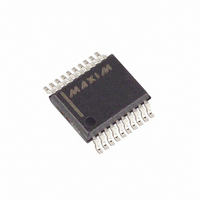
MAX3160CAP+T Maxim Integrated Products, MAX3160CAP+T Datasheet - Page 2

MAX3160CAP+T
Manufacturer Part Number
MAX3160CAP+T
Description
IC TXRX RS232/485/422 20SSOP
Manufacturer
Maxim Integrated Products
Type
Transceiverr
Datasheet
1.MAX3160CAP.pdf
(23 pages)
Specifications of MAX3160CAP+T
Number Of Drivers/receivers
2/2
Protocol
RS232, RS422, RS485
Voltage - Supply
3 V ~ 5.5 V
Mounting Type
Surface Mount
Package / Case
20-SSOP
Lead Free Status / RoHS Status
Lead free / RoHS Compliant
ABSOLUTE MAXIMUM RATINGS
V
V+ to GND ................................................................-0.3V to +7V
V- to GND....................................................................0.3V to -7V
V+ - V- (Note 1)....................................................................+13V
Input Voltages
Output Voltages
Output Short-Circuit Duration
+3.0V to+5.5V, 1µA, RS-232/RS-485/422
Multiprotocol Transceivers
Note 1: V+ and V- can have maximum magnitudes of 7V, but their absolute difference cannot exceed 13V.
Stresses beyond those listed under “Absolute Maximum Ratings” may cause permanent damage to the device. These are stress ratings only, and functional
operation of the device at these or any other conditions beyond those indicated in the operational sections of the specifications is not implied. Exposure to
absolute maximum rating conditions for extended periods may affect device reliability.
ELECTRICAL CHARACTERISTICS
(V
±10%; T
2
TRANSMITTER AND LOGIC INPUTS (DI, T1IN, T2IN, DE485, R R R R E E E E 4 4 4 4 8 8 8 8 5 5 5 5 , TE232, R R R R E E E E 2 2 2 2 3 3 3 3 2 2 2 2 , FAST, HDPLX, SHDN, RS485/R R R R S S S S 2 2 2 2 3 3 3 3 2 2 2 2 )
CC
DC CHARACTERISTICS
V
V
Logic Input Low
Logic Input High
Logic Input Leakage Current
Transmitter Logic Hysteresis
RS-232 AND RS-485/422 RECEIVER OUTPUTS (R1OUT, R2OUT, RO)
Receiver Output Voltage Low
Receiver Output Voltage High
Receiver Output Short Circuit
Current
Receiver Output Leakage
Current
CC
CC
CC
T1IN, T2IN, DI, DE485, RE485, TE232, RE232, SHDN,
FAST, HDPLX, RS485/RS232 to GND. ...............-0.3V to +6V
A, B, R1IN, R2IN to GND ...............................................±25V
T1OUT, T2OUT, Y, Z to GND......................................±13.2V
R2OUT, R1OUT, RO to GND................-0.3V to (V
T1OUT, T2OUT, Y, Z ............................................Continuous
_______________________________________________________________________________________
to GND. .............................................................-0.3V to +6V
= +3V to +5.5V, C1–C4 = 0.1µF when tested at +3.3V ±10%; C1 = 0.047µF and C2, C3, C4 = 0.33µF when tested at +5V
Standby Current
Shutdown Current
A
= T
PARAMETER
MIN
to T
MAX
, unless otherwise noted. Typical values are at T
SYMBOL
V
V
I
I
V
I
I
I
V
OSR
OZR
V
CC
CC
INL
HYS
OH
OL
IH
IL
MAX3160/MAX3161, no load,
RS485/ RS232 = GND
MAX3160/MAX3161, no load,
RS485/ RS232 = V
MAX3162 No Load
SHDN = GND, receiver inputs open or
grounded
V
V
I
I
0 < V
Receivers disabled
OUT
OUT
CC
CC
CC
= +3.3V
= +5V
= 2.5mA
= -1.5mA
O
+ 0.3V)
< V
CC
CONDITIONS
CC
Continuous Power Dissipation (T
Operating Temperature Ranges
Storage Temperature Range .............................-65°C to +150°C
Junction Temperature ......................................................+150°C
Lead Temperature (soldering, 10s) .................................+300°C
20-Pin SSOP (derate 11.9W/°C above +70°C) ..........952mW
24-Pin SSOP (derate 14.9W/°C above +70°C) ........1195mW
28-Pin SSOP (derate 15W/°C above +70°C) ...........1201mW
MAX316_CA_ ....................................................0°C to +70°C
MAX316_EA_ .................................................-40°C to +85°C
A
= +25°C.)
V
CC
MIN
2.0
2.4
- 0.6
A
= +70°C)
±0.01
±0.05
TYP
±20
1.2
2.5
3.0
0.5
1
MAX
±60
2.5
5.5
0.8
0.4
10
±1
±1
6
UNITS
mA
mA
µA
µA
µA
V
V
V
V
V


