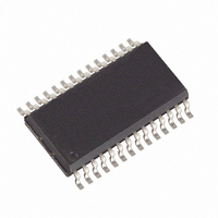
MAX3535EEWI+T Maxim Integrated Products, MAX3535EEWI+T Datasheet - Page 23

MAX3535EEWI+T
Manufacturer Part Number
MAX3535EEWI+T
Description
IC TXRX RS485/422 28-SOIC
Manufacturer
Maxim Integrated Products
Type
Transceiverr
Datasheet
1.MXL1535ECWI.pdf
(25 pages)
Specifications of MAX3535EEWI+T
Number Of Drivers/receivers
1/1
Protocol
RS422, RS485
Voltage - Supply
3 V ~ 5.5 V
Mounting Type
Surface Mount
Package / Case
28-SOIC (7.5mm Width)
Lead Free Status / RoHS Status
Lead free / RoHS Compliant
The Machine Model for ESD tests all pins using a
200pF storage capacitor and zero discharge resis-
tance. Its objective is to simulate the stress caused by
contact that occurs with handling and assembly during
manufacturing. All pins require this protection during
manufacturing, not just inputs and outputs. Therefore,
after PC board assembly, the Machine Model is less
relevant to I/O ports.
The self-oscillation circuit shown in Figure 5 is an excel-
lent way to get an approximate measure of the speed
of the MAX3535E/MXL1535E. An oscillation frequency
of 250kHz in this configuration implies a data rate of at
least 500kbps for the receiver and transmitter com-
bined. In practice, data can usually be sent and
received at a considerably higher data rate, normally
limited by the allowable jitter and data skew. If the sys-
tem can tolerate a 25% data skew, (the difference
between t
specification implies a data rate of 877kbps. Lower
data rates result in less distortion and jitter (Figure 16).
Figure 15. Human Body Current Waveform
AMPERES
+3V to +5V, 2500V
I
P
36.8%
100%
90%
10%
PLH1
0
0
t
RL
and t
Transceivers with ±15kV ESD Protection
______________________________________________________________________________________
PHL1
CURRENT WAVEFORM
TIME
), the 285ns maximum jitter
t
DL
I r
PEAK-TO-PEAK RINGING
(NOT DRAWN TO SCALE)
Machine Model
RMS
Skew
Isolated RS-485/RS-422
Higher rates are possible but with more distortion and
jitter. The data rate should always be limited below
1.75Mbps for both receiver and driver to avoid interfer-
ence with the internal barrier communication.
The MAX3535E/MXL1535E pin configurations enable
optimal PC board layout by minimizing interconnection
lengths and crossovers:
• For maximum isolation, the isolation barrier should not
• A shield trace connected to the ground on each side of
• Try to maximize the width of the isolation barrier
Figure 16. Data Skew vs. Data Rate Graph
be breached except by the MAX3535E/MXL1535E and
the transformer. Connections and components from
one side of the barrier should not be located near those
of the other side of barrier.
the barrier can help intercept capacitive currents that
might otherwise couple into the DI and SLO inputs. In a
double-sided or multilayer board, these shield traces
should be present on all conductor layers.
wherever possible. A clear space of at least 0.25in
between GND1 and GND2 is recommended.
50
45
40
35
30
25
20
15
10
5
0
0
250
DATA SKEW vs. DATA RATE
500 750
DATA RATE (kbps)
Layout Considerations
1000 1250 1500 1750 2000
TYP SKEW
MAX SKEW
23


