ESD7004MUTAG ON Semiconductor, ESD7004MUTAG Datasheet
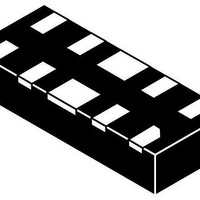
TVS Diodes - Transient Voltage Suppressors Low Capacitance ESD Protection Diode

ESD7004MUTAG

Manufacturer Part Number
ESD7004MUTAG
Description
TVS Diodes - Transient Voltage Suppressors Low Capacitance ESD Protection Diode
Manufacturer
ON Semiconductor
Series
-r
Datasheet

Specifications of ESD7004MUTAG

Polarity
Unidirectional
Channels
4 Channels
Clamping Voltage
10 V
Package / Case
UDFN-10
Breakdown Voltage
5.5 V
Termination Style
SMD/SMT
Capacitance
0.4 pF
Maximum Operating Temperature
+ 125 C
Minimum Operating Temperature
- 55 C
Dimensions
1 mm W x 2.5 mm L x 0.55 mm H
Mounting Style
SMD/SMT
Voltage - Reverse Standoff (typ)
5V
Voltage - Breakdown
5.5V
Power (watts)
-
Polarization
4 Channel Array - Unidirectional
Mounting Type
Surface Mount
Rohs Compliant
YES
Diode Type
Low Capacitance / ESD Protection
Clamping Voltage Vc Max
15.6V
Diode Case Style
UDFN
No. Of Pins
10
Svhc
No SVHC (20-Jun-2011)
Lead Free Status / Rohs Status
 Details

Available stocks

Company
Part Number
Manufacturer
Quantity
Price
Part Number:
ESD7004MUTAG
Manufacturer:
ON
Quantity:
69 900
Part Number:
ESD7004MUTAG
Manufacturer:
ON Semiconductor
Quantity:
1 950
Part Number:
ESD7004MUTAG
Manufacturer:
ON/安森美
Quantity:
20 000
Part Number:
ESD7004MUTAG
Manufacturer:
ON
Quantity:
15 957
Company:
Part Number:
ESD7004MUTAG
Quantity:
2 500
Company:
Part Number:
ESD7004MUTAG
Quantity:
30 000
ESD7004
Transient Voltage
Suppressors
Low Capacitance ESD Protection Diode
for High Speed Data Line
high speed data lines from ESD. Ultra−low capacitance and low ESD
clamping voltage make this device an ideal solution for protecting
voltage sensitive high speed data lines. The flow−through style
package allows for easy PCB layout and matched trace lengths
necessary to maintain consistent impedance between high speed
differential lines such as USB 3.0 and HDMI.
Features
Typical Applications
Stresses exceeding Maximum Ratings may damage the device. Maximum
Ratings are stress ratings only. Functional operation above the Recommended
Operating Conditions is not implied. Extended exposure to stresses above the
Recommended Operating Conditions may affect device reliability.
See Application Note AND8308/D for further description of
survivability specs.
MAXIMUM RATINGS
© Semiconductor Components Industries, LLC, 2011
April, 2011 − Rev. 2
Operating Junction Temperature Range
Storage Temperature Range
Lead Solder Temperature −
Maximum (10 Seconds)
IEC 61000−4−2 Contact (ESD)
IEC 61000−4−2 Air (ESD)
The ESD7004 transient voltage suppressor is designed to protect
IEC 61000−4−2 (Level 4)
Low Capacitance (0.4 pF Typical, I/O to GND)
Protection for the Following IEC Standards:
Low ESD Clamping Voltage
This is a Pb−Free Device
USB 3.0
HDMI
Display Port
eSATA
Rating
(T
J
= 25°C unless otherwise noted)
Symbol
ESD
ESD
T
T
T
stg
J
L
−55 to +125
−55 to +150
Value
260
±15
±15
1
Unit
°C
°C
°C
kV
kV
†For information on tape and reel specifications,
ESD7004MUTAG
including part orientation and tape sizes, please
refer to our Tape and Reel Packaging Specification
Brochure, BRD8011/D.
(*Note: Microdot may be in either location)
Device
4M
M
G
ORDERING INFORMATION
N/C N/C
I/O
10
PIN CONFIGURATION
1
Pin 1
http://onsemi.com
AND SCHEMATIC
= Specific Device Code (tbd)
= Date Code
= Pb−Free Package
CASE 517BB
I/O
9
2
UDFN10
Pin 2
=
Pins 3, 8
(Pb−Free)
GND
GND
Package
UDFN10
8
3
Publication Order Number:
Pin 4
N/C N/C
I/O
7
4
Pin 5
I/O
MARKING
DIAGRAM
Tape & Reel
Shipping
6
5
ESD7004/D
3000 /
4M MG
G

Related parts for ESD7004MUTAG

ESD7004MUTAG Summary of contents

Page 1

... I/O GND I/O I/O Pin 1 Pin 2 Pin 4 Pin 5 Pins ORDERING INFORMATION Device Package Shipping ESD7004MUTAG UDFN10 3000 / (Pb−Free) Tape & Reel including part orientation and tape sizes, please refer to our Tape and Reel Packaging Specification Brochure, BRD8011/D. Publication Order Number: ESD7004/D G ...

Page 2

ELECTRICAL CHARACTERISTICS (T Parameter Symbol Reverse Working Voltage V RWM Breakdown Voltage V BR Reverse Leakage Current I R Clamping Voltage (Note Clamping Voltage (Note Clamping Voltage V C TLP (Note 3) See Figures ...

Page 3

... ON Semiconductor has developed a way to examine the entire voltage waveform across the ESD protection diode over the time domain of an ESD pulse in the form of an oscilloscope screenshot, which can be found on the datasheets for all ESD protection diodes ...

Page 4

VOLTAGE (V) Figure 6. Positive TLP I−V Curve Transmission Line Pulse (TLP) Measurement Transmission Line Pulse (TLP) provides current versus voltage ...

Page 5

Without ESD Figure 10. USB3.0 Eye Diagram with and without ESD7004. 5.0 Gb/s, 400 mV Without ESD Figure 11. HDMI1.4 Eye Diagram with and without ESD7004. 3.4 Gb/s, 400 mV Without ESD Figure 12. ESATA3.0 Eye Diagram with and without ...

Page 6

Test Board Region TDR max = 92 USB spec requirement ± 10% Figure 13. USB TDR Measurement Differential Impedance Target, 200 ps Rise Time Test Board Region ** HDMI spec requirement is 100 ...

Page 7

ESD7004 IO−GND −8 ESD7004 IO−IO −10 1.E+06 1.E+07 1.E+08 FREQUENCY (Hz) Figure 15. ESD7004 Insertion Loss ESD7004 Figure 16. USB3.0 Layout Diagram http://onsemi.com 7 1.E+09 1.E+10 USB 3.0 Type A Connector StdA_SSTX+ Vbus StdA_SSTX− ...

Page 8

ESD7004 ESD7004 N/C (or HEC_DAT – HDMI1.4) HPD (and HEC_DAT – HDMI1.4) NUP4114 Figure 17. HDMI Layout Diagram e S ATA Connector GND A+ ESD7004 A− GND B− B+ GND Figure 18. eSATA Layout Diagram http://onsemi.com 8 HDMI Type A ...

Page 9

... B OUTLINE 0.05 C NOTE 3 *For additional information on our Pb−Free strategy and soldering details, please download the ON Semiconductor Soldering and Mounting Techniques Reference Manual, SOLDERRM/D. N. American Technical Support: 800−282−9855 Toll Free USA/Canada Europe, Middle East and Africa Technical Support: Phone: 421 33 790 2910 Japan Customer Focus Center Phone: 81− ...

Related keywords