DS2181AQ Maxim Integrated Products, DS2181AQ Datasheet - Page 7
DS2181AQ
Manufacturer Part Number
DS2181AQ
Description
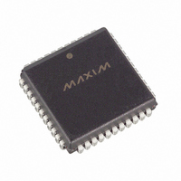
IC TXRX CEPT PRIMARY RATE 44PLCC
Manufacturer
Maxim Integrated Products
Type
Transceiverr
Datasheet
1.DS2181A.pdf
(32 pages)
Specifications of DS2181AQ
Number Of Drivers/receivers
1/1
Protocol
CEPT
Voltage - Supply
4.5 V ~ 5.5 V
Mounting Type
Surface Mount
Package / Case
44-LCC, 44-PLCC
Lead Free Status / RoHS Status
Contains lead / RoHS non-compliant
Available stocks
Company
Part Number
Manufacturer
Quantity
Price
Company:

Part Number:
DS2181AQ
Manufacturer:
Dallas
Quantity:
5 631
Part Number:
DS2181AQ
Manufacturer:
DALLAS
Quantity:
20 000
Company:
Part Number:
DS2181AQ+
Manufacturer:
Maxim Integrated Products
Quantity:
135
Company:
Part Number:
DS2181AQ+
Manufacturer:
Maxim
Quantity:
28
Company:
Part Number:
DS2181AQ+T&R
Manufacturer:
Maxim Integrated
Quantity:
10 000
Company:
Part Number:
DS2181AQ/T&R
Manufacturer:
Maxim Integrated
Quantity:
10 000


ADDRESS/COMMAND
An address/command byte write must precede any read or write of the port registers. The first bit written
(LSB) of the address/command byte specifies read or write. The following nibble identifies register
address. The next 2 bits are reserved and must be set to 0 for proper operation. The last bit of the
address/command word enables the burst mode when set; the burst mode allows consecutive reading or
writing of all register data. Data is written to and read from the port LSB first.
CHIP SELECT AND CLOCK CONTROL
All data transfers are initiated by driving the
Data is output on the falling edge of SCLK and held to the next falling edge. All data transfers are
terminated and SDO tri-stated when
CLOCKS
To access the serial port registers both TCLK and RCLK are required along with the SCLK. The TCLK
and RCLK are used to internally access the transmit and receive registers, respectively. The CCR is
considered a receive register for this purpose.
DATA I/O
Following the eight SCLK cycles that input the address/ command byte, data at SDI is strobed into the
addressed register on the next eight SCLK cycles (register write) or data is presented at SDO on the next
eight SCLK cycles (register read). SDO is tri-stated during writes and may be tied to SDI in applications
where the host processor has bi-directional I/O capability.
BURST MODE
The burst mode allows all on-chip registers to be consecutively read or written by the host processor. This
feature minimizes device initialization time on system power-up or reset. Burst mode is initiated when
ACB.7 is set and the address nibble is 0000. All registers must be read or written during the burst mode.
If
ACB: ADDRESS COMMAND BYTE Figure 2
(MSB)
SYMBOL
CS
BM
ADD3
ADD2
ADD1
ADD0
R/W
BM
transitions high before the burst is complete, data validity is not guaranteed.
-
-
-
POSITION
ACB.7
ACB.6
ACB.5
ACB.4
ACB.3
ACB.2
ACB.1
ACB.0
-
CS
NAME AND DESCRIPTION
Burst Mode. If set (and ACB.1 through ACB.4=0) burst read or
write is enabled.
Reserved, must be 0 for proper operation.
Reserved, must be 0 for proper operation.
MSB of register address.
LSB of register address.
Read/Write Select.
0 = write addressed register.
1 = read addressed register.
returns to high.
ADD3
CS
input low. Data is sampled on the rising edge of SCLK.
7 of 32
ADD2
ADD1
AD0
(LSB)
DS2181A
R/
W
Related parts for DS2181AQ
Image
Part Number
Description
Manufacturer
Datasheet
Request
R

Part Number:
Description:
MAX7528KCWPMaxim Integrated Products [CMOS Dual 8-Bit Buffered Multiplying DACs]
Manufacturer:
Maxim Integrated Products
Datasheet:
Part Number:
Description:
Single +5V, fully integrated, 1.25Gbps laser diode driver.
Manufacturer:
Maxim Integrated Products
Datasheet:
Part Number:
Description:
Single +5V, fully integrated, 155Mbps laser diode driver.
Manufacturer:
Maxim Integrated Products
Datasheet:
Part Number:
Description:
VRD11/VRD10, K8 Rev F 2/3/4-Phase PWM Controllers with Integrated Dual MOSFET Drivers
Manufacturer:
Maxim Integrated Products
Datasheet:
Part Number:
Description:
Highly Integrated Level 2 SMBus Battery Chargers
Manufacturer:
Maxim Integrated Products
Datasheet:
Part Number:
Description:
Current Monitor and Accumulator with Integrated Sense Resistor; ; Temperature Range: -40°C to +85°C
Manufacturer:
Maxim Integrated Products
Part Number:
Description:
TSSOP 14/A�/RS-485 Transceivers with Integrated 100O/120O Termination Resis
Manufacturer:
Maxim Integrated Products
Part Number:
Description:
TSSOP 14/A�/RS-485 Transceivers with Integrated 100O/120O Termination Resis
Manufacturer:
Maxim Integrated Products
Part Number:
Description:
QFN 16/A�/AC-DC and DC-DC Peak-Current-Mode Converters with Integrated Step
Manufacturer:
Maxim Integrated Products
Part Number:
Description:
TDFN/A/65V, 1A, 600KHZ, SYNCHRONOUS STEP-DOWN REGULATOR WITH INTEGRATED SWI
Manufacturer:
Maxim Integrated Products
Part Number:
Description:
Integrated Temperature Controller f
Manufacturer:
Maxim Integrated Products
Part Number:
Description:
SOT23-6/I�/45MHz to 650MHz, Integrated IF VCOs with Differential Output
Manufacturer:
Maxim Integrated Products
Part Number:
Description:
SOT23-6/I�/45MHz to 650MHz, Integrated IF VCOs with Differential Output
Manufacturer:
Maxim Integrated Products
Part Number:
Description:
EVALUATION KIT/2.4GHZ TO 2.5GHZ 802.11G/B RF TRANSCEIVER WITH INTEGRATED PA
Manufacturer:
Maxim Integrated Products
Part Number:
Description:
QFN/E/DUAL PCIE/SATA HIGH SPEED SWITCH WITH INTEGRATED BIAS RESISTOR
Manufacturer:
Maxim Integrated Products
Datasheet: