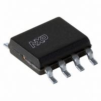
TJA1040T/N1,112 NXP Semiconductors, TJA1040T/N1,112 Datasheet - Page 4

TJA1040T/N1,112
Manufacturer Part Number
TJA1040T/N1,112
Description
IC CAN TRANSCEIVER HS 8-SOIC
Manufacturer
NXP Semiconductors
Type
Transceiverr
Datasheet
1.TJA1040TVM118.pdf
(17 pages)
Specifications of TJA1040T/N1,112
Package / Case
8-SOIC (3.9mm Width)
Number Of Drivers/receivers
1/1
Protocol
CAN
Voltage - Supply
4.75 V ~ 5.25 V
Mounting Type
Surface Mount
Product
Controller Area Network (CAN)
Number Of Transceivers
1
Data Rate
1 MBd
Supply Voltage (max)
5.25 V
Supply Voltage (min)
4.75 V
Supply Current (max)
70 mA
Maximum Operating Temperature
+ 150 C
Minimum Operating Temperature
- 40 C
Mounting Style
SMD/SMT
Lead Free Status / RoHS Status
Lead free / RoHS Compliant
Other names
935268735112
TJA1040TD
TJA1040TD
TJA1040TD
TJA1040TD
Philips Semiconductors
FUNCTIONAL DESCRIPTION
Operating modes
The TJA1040 provides two modes of operation which are
selectable via pin STB. See Table 1 for a description of the
modes of operation.
Table 1 Operating modes
N
In this mode the transceiver is able to transmit and receive
data via the bus lines CANH and CANL. See Fig.1 for the
block diagram. The differential receiver converts the
analog data on the bus lines into digital data which is
output to pin RXD via the multiplexer (MUX). The slope of
the output signals on the bus lines is fixed and optimized
in a way that lowest ElectroMagnetic Emission (EME) is
guaranteed.
S
In this mode the transmitter and receiver are switched off,
and the low-power differential receiver will monitor the bus
lines. A HIGH level on pin STB activates this low-power
receiver and the wake-up filter, and after t
the CAN bus is reflected on pin RXD.
The supply current on V
such a way that ElectroMagnetic Immunity (EMI) is
guaranteed and a wake-up event on the bus lines will be
recognized.
In this mode the bus lines are terminated to ground to
reduce the supply current (I
added in series with the high-side driver of RXD to prevent
a reverse current from RXD to V
In normal mode this diode is bypassed. This diode is not
bypassed in standby mode to reduce current consumption.
Split circuit
Pin SPLIT provides a DC stabilized voltage of 0.5V
turned on only in normal mode. In standby mode pin SPLIT
is floating. The V
recessive common-mode voltage by connecting pin SPLIT
2003 Oct 14
normal
standby
TANDBY MODE
ORMAL MODE
MODE
High speed CAN transceiver
HIGH
LOW
STB
PIN
SPLIT
bus dominant
wake-up request
detected
circuit can be used to stabilize the
CC
LOW
is reduced to a minimum in
CC
) to a minimum. A diode is
CC
in the unpowered state.
PIN RXD
bus recessive
no wake-up
request detected
BUS
HIGH
the state of
CC
. It is
4
to the centre tap of the split termination (see Fig.4). In case
of a recessive bus voltage <0.5V
an unsupplied transceiver in the network with a significant
leakage current from the bus lines to ground, the split
circuit will stabilize this recessive voltage to 0.5V
start of transmission does not cause a step in the
common-mode signal which would lead to poor
ElectroMagnetic Emission (EME) behaviour.
Wake-up
In the standby mode the bus lines are monitored via a
low-power differential comparator. Once the low-power
differential comparator has detected a dominant bus level
for more than t
Over-temperature detection
The output drivers are protected against over-temperature
conditions. If the virtual junction temperature exceeds the
shutdown junction temperature T
be disabled until the virtual junction temperature becomes
lower than T
By including the TXD condition, the occurrence of output
driver oscillation due to temperature drifts is avoided.
TXD dominant time-out function
A ‘TXD dominant time-out’ timer circuit prevents the bus
lines from being driven to a permanent dominant state
(blocking all network communication) if pin TXD is forced
permanently LOW by a hardware and/or software
application failure. The timer is triggered by a negative
edge on pin TXD.
If the duration of the LOW level on pin TXD exceeds the
internal timer value (t
driving the bus lines into a recessive state. The timer is
reset by a positive edge on pin TXD. The TXD dominant
time-out time t
40 kBaud.
Fail-safe features
Pin TXD provides a pull-up towards V
recessive level in case pin TXD is unsupplied.
Pin STB provides a pull-up towards V
the transceiver into standby mode in case pin STB is
unsupplied.
In the event that the V
will become floating to prevent reverse supplying
conditions via these pins.
j(sd)
dom
BUS
and TXD becomes recessive again.
defines the minimum possible bit rate of
, pin RXD will become LOW.
dom
CC
), the transmitter is disabled,
is lost, pins TXD, STB and RXD
CC
j(sd)
due to the presence of
, the output drivers will
Product specification
CC
CC
in order to force a
in order to force
TJA1040
CC
. So a


