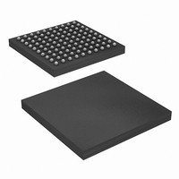
CYP15G0101DXB-BBXI Cypress Semiconductor Corp, CYP15G0101DXB-BBXI Datasheet - Page 28

CYP15G0101DXB-BBXI
Manufacturer Part Number
CYP15G0101DXB-BBXI
Description
IC TXRX HOTLINK 100-LBGA
Manufacturer
Cypress Semiconductor Corp
Series
HOTlink II™r
Type
Transceiverr
Datasheet
1.CYP15G0101DXB-BBXC.pdf
(44 pages)
Specifications of CYP15G0101DXB-BBXI
Package / Case
100-LBGA
Protocol
Fibre Channel
Voltage - Supply
3.135 V ~ 3.465 V
Mounting Type
Surface Mount
Product
PHY
Data Rate
1500 MBd
Supply Voltage (max)
3.465 V
Supply Voltage (min)
3.135 V
Supply Current
0.51 A
Maximum Operating Temperature
+ 85 C
Minimum Operating Temperature
- 40 C
Mounting Style
SMD/SMT
Number Of Channels
1
Lead Free Status / RoHS Status
Lead free / RoHS Compliant
For Use With
CYP15G0101DX-EVAL - EVAL BRD FOR HOTLINK II
Number Of Drivers/receivers
-
Lead Free Status / Rohs Status
Lead free / RoHS Compliant
Available stocks
Company
Part Number
Manufacturer
Quantity
Price
Company:
Part Number:
CYP15G0101DXB-BBXI
Manufacturer:
SPANSION
Quantity:
1 200
Company:
Part Number:
CYP15G0101DXB-BBXI
Manufacturer:
Cypress Semiconductor Corp
Quantity:
10 000
Part Number:
CYP15G0101DXB-BBXI
Manufacturer:
CYPRESS/赛普拉斯
Quantity:
20 000
CYP(V)(W)15G0101DXB AC Characteristics
Over the Operating Range (continued)
Document Number: 38-02031 Rev. *L
t
t
t
t
t
t
t
Transmit Serial Outputs and TX PLL Characteristics
t
t
t
t
t
t
Receive Serial Inputs and CDR PLL Characteristics
t
t
t
t
Capacitance
C
C
Notes
RREFDA
RREFDV
REFDV–
REFDV+
REFCDV–
REFCDV+
REFRX
B
RISE
FALL
DJ
RJ
TXLOCK
RXLOCK
RXUNLOCK
JTOL
DJTOL
44. REFCLK has no phase or frequency relationship with the recovered clock(s) and only acts as a centering reference to reduce clock synchronization time. REFCLK
45. Tested initially and after any design or process changes that may affect these parameters, but not 100% tested.
46. Since this timing parameter is greater than the minimum time period of REFCLK it sets an upper limit to the frequency in which REFCLKx can be used to clock
47. This parameter is 649 ps for CYW15G0101DXB.
48. While sending continuous K28.5s, outputs loaded to a balanced 100 load, measured at the cross point of the differential outputs over the operating range.
49. While sending continuous K28.7s, after 100,000 samples measured at the cross point of differential outputs, time referenced to REFCLK input, over the operating
50. Total jitter is calculated at an assumed BER of 1E
51. Also meets all Jitter Generation and Jitter Tolerance requirements as specified by SMPTE 259M, SMPTE 292M, OBSAI RP3, CPRI, ESCON, FICON, Fibre
52. Receiver UI (Unit Interval) is calculated as 1/(f
INTTL
INPECL
Parameter
[45, 48, 50]
[45, 49, 50]
Parameter
must be within ±1500 ppm (±0.15%) of the remote transmitter’s PLL reference (REFCLK) frequency. Although transmitting to a HOTLink II receiver necessitates
the frequency difference between the transmitter and receiver reference clocks to be within ±1500 ppm, the stability of the crystal needs to be within the limits
specified by the appropriate standard when transmitting to a remote receiver that is compliant to that standard. For example, to be IEEE 802.3z Gigabit Ethernet
compliant, the frequency stability of the crystal needs to be within ±100 ppm.
the receive data out of the output register. For predictable timing, users can use this parameter only if REFCLK period is greater than sum of t
time of the upstream device. When this condition is not true, RXCLKC± or RXCLKA± (a buffered or delayed version of REFCLK when RXCKSELx = LOW) could
be used to clock the receive data out of the device.
range.
Channel and DVB-ASI.
RXRATE = HIGH) or 1/(f
[45]
[45]
[50]
[50]
[44, 45]
[46]
[45]
Receive data access time from REFCLK (RXCKSEL LOW)
Receive data valid time from REFCLK(RXCKSEL LOW)
Received data valid time to RXCLK (RXCKSEL = LOW)
Received data valid time from RXCLK (RXCKSEL = LOW)
Received data valid time to RXCLKC (RXCKSEL = LOW)
Received data valid time from RXCLKC (RXCKSEL = LOW)
REFCLK frequency referenced to extracted received clock frequency
Bit time
CML output rise time 20%–80% (CML test load)
CML output fall time 80%–20% (CML test load)
Deterministic Jitter (peak-peak)
Random Jitter ()
Transmit PLL lock to REFCLK
Receive PLL lock to input data stream (cold start)
Receive PLL lock to input data stream
Receive PLL unlock rate
Total jitter tolerance
Deterministic jitter tolerance
TTL input capacitance
PECL input capacitance
REF
* 10) (when RXRATE = LOW) of the remote transmitter if data is being received. In an operating link this is equivalent to t
REF
Description
* 20) (when RXRATE = HIGH) or 1/(f
12. Hence: Total Jitter (t
Description
J
)
=
REF
(t
RJ
* 10) (when RXRATE = LOW) if no data is being received, or 1/(f
* 14) + t
T
T
A
A
= 25 °C, f
= 25 °C, f
SPDSEL = HIGH
SPDSEL = HIGH
SPDSEL = LOW
SPDSEL = LOW
DJ
SPDSEL = MID
SPDSEL = MID
IEEE 802.3z
IEEE 802.3z
IEEE 802.3z
IEEE 802.3z
.
Test Conditions
0
0
= 1 MHz, V
= 1 MHz, V
[51]
[51]
[51]
[51]
CC
CC
10UI – 4.7
10UI – 4.3
–1500
= 3.3 V
5100
= 3.3 V
–0.2
Min
100
180
100
180
600
370
CYW15G0101DXB
2.5
0.5
60
60
CYP15G0101DXB
CYV15G0101DXB
–
–
–
–
–
–
–
+1500
666
376K
376K
1000
1000
RREFDA
Max
Max
270
500
270
500
200
9.5
25
46
B
11
–
–
–
–
–
–
–
7
4
[47]
REF
Page 28 of 44
and set-up
* 20)(when
UI
Unit
ppm
Unit
pF
pF
ns
ns
ns
ns
ns
ns
ps
ps
ps
ps
ps
ps
ps
ps
ps
us
UI
UI
ps
ps
[52]
[+] Feedback


