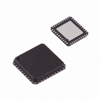
ADV7179BCPZ Analog Devices Inc, ADV7179BCPZ Datasheet - Page 40

ADV7179BCPZ
Manufacturer Part Number
ADV7179BCPZ
Description
IC ENCODER VID NTSC/PAL 40LFCSP
Manufacturer
Analog Devices Inc
Type
Video Encoderr
Datasheet
1.ADV7179KCPZ.pdf
(52 pages)
Specifications of ADV7179BCPZ
Applications
Digital Cameras, Mobile Phones, Portable Video
Voltage - Supply, Analog
2.8 V, 3.3 V
Mounting Type
Surface Mount
Package / Case
40-LFCSP
Input Format
Digital
Output Format
Analog
Supply Voltage Range
3V To 3.6V
Operating Temperature Range
-40°C To +85°C
Tv / Video Case Style
LFCSP
No. Of Pins
40
Msl
MSL 1 - Unlimited
Lead Free Status / RoHS Status
Lead free / RoHS Compliant
Voltage - Supply, Digital
-
Lead Free Status / RoHS Status
Lead free / RoHS Compliant, Lead free / RoHS Compliant
Available stocks
Company
Part Number
Manufacturer
Quantity
Price
Company:
Part Number:
ADV7179BCPZ
Manufacturer:
ADI
Quantity:
230
Part Number:
ADV7179BCPZ
Manufacturer:
ADI/亚德诺
Quantity:
20 000
Company:
Part Number:
ADV7179BCPZ-REEL
Manufacturer:
XILINX
Quantity:
1 150
ADV7174/ADV7179
SUPPLY DECOUPLING
For optimum performance, bypass capacitors should be in-
stalled using the shortest leads possible, consistent with reliable
operation, to reduce the lead inductance. Best performance is
obtained with 0.1 μF ceramic capacitor decoupling. Each group
of V
0.1 μF decoupling capacitor to GND. These capacitors should
be placed as close to the device as possible.
It is important to note that while the ADV7174/ADV7179
contains circuitry to reject power supply noise, this rejection
decreases with frequency. If a high frequency switching power
supply is used, the designer should pay close attention to
reducing power supply noise and consider using a 3-terminal
voltage regulator for supplying power to the analog power
plane.
DIGITAL SIGNAL INTERCONNECT
The digital inputs to the ADV7174/ADV7179 should be
isolated as much as possible from the analog outputs and other
analog circuitry. Also, these input signals should not overlay the
analog power plane.
Due to the high clock rates involved, long clock lines to the
ADV7174/ADV7179 should be avoided to reduce noise pickup.
Any active termination resistors for the digital inputs should be
connected to the regular PCB power plane (V
analog power plane.
AA
pins on the ADV7174/ADV7179 must have at least one
HSYNC
CLOCK
CC
D
) and not to the
CK
Figure 55. Circuit to Generate 13.5 MHz
Q
Rev. B | Page 40 of 52
ANALOG SIGNAL INTERCONNECT
The ADV7174/ADV7179 should be located as close to the
output connectors as possible to minimize noise pickup and
reflections due to impedance mismatch.
The video output signals should overlay the ground plane, not
the analog power plane, to maximize the high frequency power
supply rejection.
Digital inputs, especially pixel data inputs and clocking signals,
should never overlay any of the analog signal circuitry and
should be kept as far away as possible.
For best performance, the outputs should each have a 75 Ω load
resistor connected to GND. These resistors should be placed as
close as possible to the ADV7174/ADV7179 to minimize
reflections.
The ADV7174/ADV7179 should have no inputs left floating.
Any inputs that are not required should be tied to ground.
The circuit in Figure 55 can be used to generate a 13.5 MHz
waveform using the 27 MHz clock and the HSYNC pulse. This
waveform is guaranteed to produce the 13.5 MHz clock in
synchronization with the 27 MHz clock. This 13.5 MHz clock
can be used if the 13.5 MHz clock is required by the MPEG
decoder. This guarantees that the Cr and Cb pixel information
is input to the ADV7174/ADV7179 in the correct sequence.
Note that the exposed metal paddle on the bottom side of the
LFCSP package must be soldered to PCB ground for proper
heat dissipation and also for electrical noise and mechanical
strength benefits.
D
CK
Q
13.5MHz


