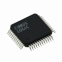
CS4954-CQZ Cirrus Logic Inc, CS4954-CQZ Datasheet - Page 32

CS4954-CQZ
Manufacturer Part Number
CS4954-CQZ
Description
IC VIDEO ENCODER NTSC/PAL 48TQFP
Manufacturer
Cirrus Logic Inc
Type
Video Encoderr
Datasheet
1.CS4954-CQZ.pdf
(60 pages)
Specifications of CS4954-CQZ
Package / Case
48-TQFP, 48-VQFP
Voltage - Supply, Analog
3.15 V ~ 5.25 V
Voltage - Supply, Digital
3.15 V ~ 5.25 V
Mounting Type
Surface Mount
Operating Supply Voltage
3.3 V / 5 V
Supply Current
70 mA
Maximum Operating Temperature
+ 85 C
Minimum Operating Temperature
- 40 C
Mounting Style
SMD/SMT
Number Of Channels
2
Resolution
10 bit
Snr
70 dB
Input Format
Digital
Output Format
Analog
Supply Voltage Range
3.15V To 3.45V
Operating Temperature Range
-40°C To +85°C
Tv / Video Case Style
TQFP
No. Of Pins
48
Tv / Video Type
Encoder
Rohs Compliant
Yes
Filter Terminals
SMD
Lead Free Status / RoHS Status
Lead free / RoHS Compliant
For Use With
CDB4955A - EVALUATION BOARD FOR CS4955A
Applications
-
Lead Free Status / Rohs Status
Lead free / RoHS Compliant
Other names
598-1682
Available stocks
Company
Part Number
Manufacturer
Quantity
Price
Part Number:
CS4954-CQZ
Manufacturer:
CIRRUS
Quantity:
20 000
Company:
Part Number:
CS4954-CQZR
Manufacturer:
NXP
Quantity:
11 000
Company:
Part Number:
CS4954-CQZR
Manufacturer:
Cirrus Logic Inc
Quantity:
10 000
Part Number:
CS4954-CQZR
Manufacturer:
CIRRUS
Quantity:
20 000
7.
7.1
All CS4954/5 analog timing and sequencing is de-
rived from the 27 MHz clock input. The analog out-
puts are controlled internally by the video timing
generator in conjunction with master and slave tim-
ing.
Since the CS4954/5 is almost entirely a digital cir-
cuit, great care has been taken to guarantee analog
timing and slew rate performance as specified in
the NTSC and PAL analog specifications. Refer-
ence the Analog Parameters section of this data
sheet for the performance specifications.
7.2
The CS4954/5 can operate with or without the aid
of an external voltage reference. The CS4954/5 is
designed with an internal voltage reference genera-
tor that provides a VREFOUT signal at the VREF
pin. The internal voltage reference is utilized by not
making a connection to the VREF pin. The VREF
pin can also be connected to an external precision
1.232 volt reference, which then overrides the in-
ternal reference.
7.3
All six of the CS4954/5 digital to analog converter
DACs are output current normalized with a com-
mon ISET device pin. The DAC output current per
bit is determined by the size of the resistor connect-
ed between ISET and electrical ground. Typically a
4 KΩ, 1% metal film resistor should be used. The
ISET resistance can be changed by the user to ac-
commodate varying video output attenuation via
post filters and also to suit individual preferred per-
formance needs.
In conjunction with the ISET value, the user can
also independently vary the chroma, luma and col-
orburst amplitude levels via host addressable con-
32
ANALOG
Analog Timing
VREF
ISET
trol register bits that are used to control internal
digital amplifiers. The DAC output levels are de-
fined by the following equations:
CVBS/Y/C/R/G/B outputs in low impedance mode:
CVBS/Y/C/R/G/B outputs in high impedance mode:
7.4
The CS4954/5 is has six independent, video-grade,
current-output,
(DACs). They are 10-bit DACs operating at a
27 MHz two-times-oversampling rate. All six
DACs are disabled and default to low power mode
upon RESET. Each DAC can be individually pow-
ered down and disabled. The output-current-per-bit
of all six DACs is determined by the size of the re-
sistor connected between the ISET pin and ground.
7.4.1 Luminance DAC
The Y output pin is driven from a 10-bit 27 MHz
current output DAC that internally receives the Y,
or luminance (black and white only) or CVBS data
based on its configuration. See
“CVBS DAC” on page
signed to drive proper video levels into a 37.5 Ω
load. Reference the detailed electrical section of
this data sheet for the exact Y digital to analog AC
and DC performance data. A EN_L enable control
bit in the Control Register 5 (0×05) is provided to
enable or disable the luminance DAC. To com-
pletely disable or for low power device operation,
the luminance DAC can be totally shut down via
the SVIDLUM_PD control bit in Control Register
4 (0×04). In this mode, turn-on using the control
register will not be instantaneous.
VREF/RISET = IREF
(e.g., 1.232 V/4K Ω = 308 μA)
VOUT (max) = IREF*(16/145)*1023*37.5 Ω = 1.304V
VOUT (max) = IREF*(4/145)*1023*150Ω = 1.304 V
DACs
digital-to-analog
CS4954 CS4955
33. The Y DAC is de-
Table 1
converters
DS278F6
and


