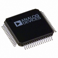
ADV7311KST Analog Devices Inc, ADV7311KST Datasheet - Page 15

ADV7311KST
Manufacturer Part Number
ADV7311KST
Description
IC VID ENC 6-12BIT DAC'S 64LQFP
Manufacturer
Analog Devices Inc
Type
Video Encoderr
Datasheet
1.ADV7311KST.pdf
(84 pages)
Specifications of ADV7311KST
Rohs Status
RoHS non-compliant
Applications
DVD, SD/HD
Voltage - Supply, Analog
2.5V
Voltage - Supply, Digital
2.5V
Mounting Type
Surface Mount
Package / Case
64-LQFP
Input Format
Digital
Output Format
Analog
Supply Voltage Range
2.375V To 2.625V
Operating Temperature Range
0°C To +70°C
Tv / Video Case Style
LQFP
No. Of Pins
64
Msl
MSL 1 - Unlimited
Lead Free Status / RoHS Status
Lead free / RoHS Compliant
Available stocks
Company
Part Number
Manufacturer
Quantity
Price
Company:
Part Number:
ADV7311KST
Manufacturer:
ADI
Quantity:
300
Company:
Part Number:
ADV7311KST
Manufacturer:
Analog Devices Inc
Quantity:
10 000
Part Number:
ADV7311KSTZ
Manufacturer:
ADI/亚德诺
Quantity:
20 000
Mnemonic
DGND
AGND
CLKIN_A
CLKIN_B
COMP1,2
DAC A
DAC B
DAC C
DAC D
DAC E
DAC F
P_HSYNC
P_VSYNC
P_BLANK
S_BLANK
S_HSYNC
S_VSYNC
Y9–Y0
C9–C0
S9–S0
RESET
R
SCLK
SDA
ALSB
V
V
V
V
EXT_LF
RTC_SCR_TR I
I
GND_IO
REV. A
2
SET1,2
DD_IO
DD
AA
REF
C
Input/Output
G
G
I
I
O
O
O
O
O
O
O
I
I
I
I/O
I/O
I/O
I
I
I
I
I
I
I/O
I
P
P
P
I/O
I
I
Pixel Clock Input for HD (74.25 MHz Only, PS Only (27 MHz), SD Only (27 MHz).
Pixel Clock Input. Requires a 27 MHz reference clock for progressive scan mode or a 74.25 MHz
Compensation Pin for DACs. Connect 0.1 F capacitor from COMP pin to V
Progressive Scan/HDTV Input Port 4:4:4 Input Mode. This port is used for the Cb[Blue/U] data.
SD or Progressive Scan/HDTV Input Port for Cr[Red/V] data in 4:4:4 input mode. LSB is set up
External Loop Filter for the Internal PLL.
Digital Input/Output Ground.
Function
Digital Ground.
Analog Ground.
(74.1758 MHz) reference clock in HDTV mode. This clock is only used in dual modes.
CVBS/Green/Y/Y Analog Output.
Chroma/Blue/U/Pb Analog Output.
Luma/Red/V/Pr Analog Output.
In SD Only Mode: CVBS/Green/Y Analog Output; in HD Only Mode and Simultaneous HD/SD
Mode: Y/Green [HD] Analog Output.
In SD Only Mode: Luma/Blue/U Analog Output; in HD Only Mode and Simultaneous HD/SD
Mode: Pr/Red Analog Output.
In SD Only Mode: Chroma/Red/V Analog Output; in HD Only Mode and Simultaneous HD/SD
Mode: Pb/Blue [HD] Analog Output.
Video Horizontal Sync Control Signal for HD in Simultaneous SD/HD Mode and HD Only Mode.
Video Vertical Sync Control Signal for HD in Simultaneous SD/HD Mode and HD Only Mode.
Video Blanking Control Signal for HD in Simultaneous SD/HD Mode and HD Only Mode.
Video Blanking Control Signal for SD Only.
Video Horizontal Sync Control Signal for SD Only.
Video Vertical Sync Control Signal for SD Only.
SD or Progressive Scan/HDTV Input Port for Y Data. Input port for interleaved progressive scan
data. The LSB is set up on Pin Y0. For 8-bit data input, LSB is set up on Y2.
The LSB is set up on pin C0. For 8-bit data input, LSB is set up on C2.
on pin S0. For 8-bit data input, LSB is set up on S2.
This input resets the on-chip timing generator and sets the ADV7310/ADV7311 into default register
setting. RESET is an active low signal.
A 3040 Ω resistor must be connected from this pin to AGND and is used to control the amplitudes
of the DAC outputs.
I
I
TTL Address Input. This signal sets up the LSB of the I
the I
Power Supply for Digital Inputs and Outputs.
Digital Power Supply.
Analog Power Supply.
Optional External Voltage Reference Input for DACs or Voltage Reference Output (1.235 V).
Multifunctional Input. Real time control (RTC) input, timing reset input, subcarrier reset input.
This input pin must be tied high (V
2
2
C Port Serial Interface Clock Input.
C Port Serial Data Input/Output.
2
C filter is activated, which reduces noise on the I
PIN FUNCTION DESCRIPTIONS
–15–
DD_IO
) for the ADV7310/ADV7311 to interface over the I
2
C interface.
2
C address. When this pin is tied low,
ADV7310/ADV7311
AA
.
2
C port.


