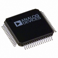
ADV7321KSTZ Analog Devices Inc, ADV7321KSTZ Datasheet - Page 63

ADV7321KSTZ
Manufacturer Part Number
ADV7321KSTZ
Description
IC VID ENC 6-12BIT DAC'S 64LQFP
Manufacturer
Analog Devices Inc
Type
Video Encoderr
Datasheet
1.ADV7321KSTZ.pdf
(88 pages)
Specifications of ADV7321KSTZ
Applications
EVD, DVD, SD/PS/HDTV
Voltage - Supply, Analog
2.5V
Voltage - Supply, Digital
2.5V
Mounting Type
Surface Mount
Package / Case
64-LQFP
Input Format
Digital
Output Format
Analog
Supply Voltage Range
2.375V To 2.625V
Operating Temperature Range
0°C To +70°C
Tv / Video Case Style
LQFP
No. Of Pins
64
Msl
MSL 1 - Unlimited
Lead Free Status / RoHS Status
Lead free / RoHS Compliant
Available stocks
Company
Part Number
Manufacturer
Quantity
Price
Company:
Part Number:
ADV7321KSTZ
Manufacturer:
Micrel
Quantity:
2 023
Company:
Part Number:
ADV7321KSTZ
Manufacturer:
ADI
Quantity:
329
Company:
Part Number:
ADV7321KSTZ
Manufacturer:
Analog Devices Inc
Quantity:
10 000
Part Number:
ADV7321KSTZ
Manufacturer:
ADI/亚德诺
Quantity:
20 000
PCB BOARD LAYOUT
The ADV7320/ADV7321 are optimally designed for lowest
noise performance of both radiated and conducted noise. To
complement the excellent noise performance of the ADV7320/
ADV7321, it is imperative that great care be given to the PC
board layout.
The layout should be optimized for lowest noise on the
ADV7320/ADV7321 power and ground lines. This can be
achieved by shielding the digital inputs and providing good
decoupling. The lead length between groups of V
V
as short as possible to minimized inductive ringing.
It is recommended that a 4-layer printed circuit board is used,
with power and ground planes separating the layer of the signal
carrying traces of the components and solder side layer. Com-
ponent placement should be carefully considered in order to
separate noisy circuits, such as crystal clocks, high speed logic
circuitry, and analog circuitry.
DD
–10
–20
–30
–40
–50
–60
–70
–80
–90
–10
–20
–30
–40
–50
–60
and DGND, and V
Figure 90. Filter Plot for Output Filter for HDTV, 2× Oversampling
0
0
1M
1M
Figure 89. Filter Plot for Output Filter for PS, 8× Oversampling
GROUP DELAY (Seconds)
GROUP DELAY (Seconds)
PHASE (Degrees)
CIRCUIT FREQUENCY RESPONSE
CIRCUIT FREQUENCY RESPONSE
10M
10M
DD_IO
FREQUENCY (Hz)
FREQUENCY (Hz)
and GND_IO pins should be kept
MAGNITUDE (dB)
100M
100M
MAGNITUDE (dB)
(Degrees)
PHASE
AA
and AGND,
1G
1G
480
400
320
240
160
80
0
–80
–160
–240
480
360
240
120
0
–120
–240
18n
16n
14n
12n
10n
8n
6n
4n
2n
0
18n
15n
12n
9n
6n
3n
0
Rev. A | Page 63 of 88
There should be a separate analog ground plane and a separate
digital ground plane.
Each power plane should encompass a digital power plane and
an analog power plane. The analog power plane should contain
the DACs and all associated circuitry, V
power plane should contain all logic circuitry.
The analog and digital power planes should be individually
connected to the common power plane at a single point
through a suitable filtering device, such as a ferrite bead.
DAC output traces on a PCB should be treated as transmission
lines. It is recommended that the DACs be placed as close as
possible to the output connector, with the analog output traces
being as short as possible (less than 3 inches). The DAC termi-
nation resistors should be placed as close as possible to the DAC
outputs and should overlay the PCB’s ground plane. As well as
minimizing reflections, short analog output traces reduce noise
pickup from neighboring digital circuitry.
To avoid crosstalk between the DAC outputs, it is recom-
mended that as much space as possible be left between the
tracks of the individual DAC output pins. The addition of
ground tracks between outputs is also recommended.
Supply Decoupling
Noise on the analog power plane can be further reduced by the
use of decoupling capacitors.
Optimum performance is achieved by the use of 10 nF and
0.1 μF ceramic capacitors. Each group of V
pins should be individually decoupled to ground. This should
be done by placing the capacitors as close as possible to the
device with the capacitor leads as short as possible, thus
minimizing lead inductance.
A 1 μF tantalum capacitor is recommended across the V
supply in addition to 10 nF ceramic. See the circuit layout in
Figure 91.
Digital Signal Interconnect
The digital signal lines should be isolated as much as possible
from the analog outputs and other analog circuitry. Digital
signal lines should not overlay the analog power plane.
Due to the high clock rates, avoid long clock lines to the
ADV7320/ADV7321 to minimize noise pickup.
Any active pull-up termination resistors for the digital inputs
should be connected to the digital power plane and not the
analog power plane.
ADV7320/ADV7321
REF
circuitry. The digital
AA
, V
DD
, or V
DD_IO
AA


