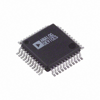
ADV7177KS Analog Devices Inc, ADV7177KS Datasheet - Page 6

ADV7177KS
Manufacturer Part Number
ADV7177KS
Description
IC DAC VIDEO NTSC 3-CH 44MQFP
Manufacturer
Analog Devices Inc
Type
Video Encoderr
Datasheet
1.ADV7177KSZ-REEL.pdf
(44 pages)
Specifications of ADV7177KS
Rohs Status
RoHS non-compliant
Applications
Set-Top Boxes, TV
Voltage - Supply, Analog
3 V ~ 3.6 V
Mounting Type
Surface Mount
Package / Case
44-MQFP, 44-PQFP
Adc/dac Resolution
9b
Screening Level
Commercial
Package Type
MQFP
Pin Count
44
Voltage - Supply, Digital
-
Lead Free Status / RoHS Status
Not Compliant
Available stocks
Company
Part Number
Manufacturer
Quantity
Price
Company:
Part Number:
ADV7177KS
Manufacturer:
AD
Quantity:
5 510
Company:
Part Number:
ADV7177KS
Manufacturer:
OMRON
Quantity:
5 510
Company:
Part Number:
ADV7177KS
Manufacturer:
ADI
Quantity:
210
Company:
Part Number:
ADV7177KSZ
Manufacturer:
Analog Devices Inc
Quantity:
10 000
Part Number:
ADV7177KSZ
Manufacturer:
ADI/亚德诺
Quantity:
20 000
Company:
Part Number:
ADV7177KSZ-REEL
Manufacturer:
Analog Devices Inc
Quantity:
10 000
Part Number:
ADV7177KSZ-REEL
Manufacturer:
ADI/亚德诺
Quantity:
20 000
ADV7177/ADV7178
3.3 V SPECIFICATIONS
V
Table 2.
Parameter
STATIC PERFORMANCE
DIGITAL INPUTS
DIGITAL OUTPUTS
ANALOG OUTPUTS
POWER REQUIREMENTS
1
2
3
4
5
6
7
8
9
10
11
The max/min specifications are guaranteed over this range. The max/min values are typical over 3.0 V to 3.6 V.
Temperature range T
Guaranteed by characterization.
All digital input pins except pins RESET , OSD0, and CLOCK.
Excluding all digital input pins except pins RESET , OSD0, and CLOCK.
Full drive into 75 Ω load.
DACs can output 35 mA typically at 3.3 V (R
Minimum drive current (used with buffered/scaled output load).
Power measurements are taken with clock frequency = 27 MHz. Max T
reduces IDAC correspondingly.
AA
I
I
DAC
CCT
Resolution (Each DAC)
Accuracy (Each DAC)
Input High Voltage, V
Input Low Voltage, V
Input Current, I
Input Current, I
Input Capacitance, C
Output High Voltage, V
Output Low Voltage, V
Three-State Leakage Current
Three-State Output Capacitance
Output Current
Output Current
DAC-to-DAC Matching
Output Compliance, V
Output Impedance, R
Output Capacitance, C
V
Normal Power Mode
Low Power Mode
Power-Supply Rejection Ratio
AA
= 3.0 V to 3.6 V
(circuit current) is the continuous current required to drive the device.
I
I
I
I
I
I
is the total current (min corresponds to 5 mA output per DAC, max corresponds to 38 mA output per DAC) to drive all three DACs. Turning off individual DACs
DAC
DAC
CCT
DAC
DAC
CCT
Integral Nonlinearity
Differential Nonlinearity
9
11
(max)
(min)
(max)
(min)
3
3
10
3
IN
IN
6, 7
8
MIN
3, 4
3, 5
3
1
, V
to T
3
INL
IN
INH
OUT
3, 9
REF
MAX
OC
OUT
OL
OH
: 0°C to 70°C.
= 1.235 V, R
3
3
SET
Guaranteed monotonic
V
V
I
I
R
I
R
Conditions
COMP = 0.1 µF
SOURCE
SINK
OUT
= 150 Ω and R
SET
IN
IN
SET
SET
= 0.4 V or 2.4 V
= 0.4 V or 2.4 V
= 0 mA
= 3.2 mA
= 300 Ω. All specifications T
= 300 Ω, R
= 300 Ω, R
= 400 µA
1
L
= 75 Ω), optimum performance obtained at 18 mA DAC current (R
L
L
= 150 Ω
= 75 Ω
J
= 110°C.
Rev. C | Page 6 of 44
MIN
Min
16.5
0
3.0
to T
MAX
2
, unless otherwise noted.
Typ
2
0.8
10
2.4
0.4
10
17.35
5
2.0
15
3.3
113
15
45
60
25
45
0.01
Max
9
±0.5
±0.5
±1
±50
10
18.5
1.4
30
3.6
116
0.5
SET
= 300 Ω and R
Unit
Bits
LSB
LSB
V
V
µA
µA
pF
V
V
µA
pF
mA
mA
%
V
kΩ
pF
V
mA
mA
mA
mA
mA
mA
%/%
L
= 150 Ω).


