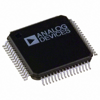
ADV7191KSTZ Analog Devices Inc, ADV7191KSTZ Datasheet - Page 34

ADV7191KSTZ
Manufacturer Part Number
ADV7191KSTZ
Description
IC ENCODER VIDEO W/DAC 64LQFP
Manufacturer
Analog Devices Inc
Type
Video Encoderr
Datasheet
1.ADV7191KST.pdf
(72 pages)
Specifications of ADV7191KSTZ
Applications
DVD, PC Video, Multimedia
Voltage - Supply, Analog
3.3 V ~ 5 V
Mounting Type
Surface Mount
Package / Case
64-LQFP
Number Of Dac's
6
Adc/dac Resolution
10b
Screening Level
Commercial
Package Type
LQFP
Pin Count
64
Lead Free Status / RoHS Status
Lead free / RoHS Compliant
Voltage - Supply, Digital
-
Lead Free Status / RoHS Status
Compliant, Lead free / RoHS Compliant
Available stocks
Company
Part Number
Manufacturer
Quantity
Price
Company:
Part Number:
ADV7191KSTZ
Manufacturer:
FUJITSU
Quantity:
92
Part Number:
ADV7191KSTZ
Manufacturer:
ADI/亚德诺
Quantity:
20 000
ADV7190/ADV7191
Reserved (MR76)
A Logic 0 must be written to this bit.
CLAMP/VSO Select (MR77)
This bit is used to select the functionality of Pin 51. A 1 selects
CLAMP as the output signal. A 0 selects VSO output.
MODE REGISTER 8
MR8 (MR87–MR80)
(Address (SR4–SR0) = 08H)
Mode Register 8 is an 8-bit-wide register. Figure 58 shows the
various operations under the control of Mode Register 8.
MR8 BIT DESCRIPTION
Reserved (MR80, MR81)
A Logic 0 must be written to these bits.
Double Buffer Control (MR82)
Double buffering can be enabled or disabled on the Contrast
Control Register, U Scale Register, V Scale Register, Hue Adjust
Control Register, Closed Captioning Register, Brightness Con-
trol Register, Gamma Curve Select Bit and the Macrovision
Registers (ADV7190 only). Double Buffering is not available in
Master Timing mode.
16-Bit Pixel Port (MR83)
This bit controls if the ADV7190/ADV7191 accepts 8-bit or
16-bit input data. In 8-bit mode the data will be input on Pins
P0–P7. Unused pixel inputs should be grounded.
Reserved (MR84)
A Logic 0 must be written to this bit.
DNR Enable Control (MR85)
To enable the DNR process this bit has to be set to 1. If this bit
is set to 0, the DNR processing is bypassed. For further infor-
mation on DNR controls see DNR Registers 2–0, DNR1 Bit
Description, and DNR2 Bit Description sections.
Gamma Enable Control (MR86)
To enable the programmable gamma correction this bit has
to be set to enabled (MR86 is set to 1). For further information
SELECT CONTROL
MR87
GAMMA CURVE
0
1
MR97
MR87
ZERO MUST
BE WRITTEN
TO THESE BITS
CURVE A
CURVE B
MR97 MR96
MR86
GAMMA ENABLE
0
1
CONTROL
MR96
MR86
DISABLE
ENABLE
MR85
MR95 MR94
0
1
DNR ENABLE
Figure 58. Mode Register 8 (MR8)
Figure 59. Mode Register 9 (MR9)
0
0
1
1
CONTROL
MR95
DELAY CONTROL
MR85
DISABLE
ENABLE
0
1
0
1
CHROMA
0ns DELAY
148ns DELAY
296ns DELAY
RESERVED
ZERO MUST
BE WRITTEN
TO THIS BIT
MR94
MR84
MR84
MR83
–34–
0
1
16-PIXEL PORT
8-BIT PIXEL PORT
16-BIT PIXEL PORT
on Gamma Correction controls see Gamma Correction Registers
0–13 (Gamma 0–13) (Address (SR5–SR0) = 26H–32H) section.
Gamma Curve Select Control (MR87)
This bit selects which of the two programmable gamma curves is
used. When setting MR87 to 0, the gamma correction curve to be
processed is Curve A. Otherwise, Curve B is selected. For fur-
ther information on Gamma Correction controls see Gamma
Correction Registers 0–13 (Gamma 0–13) (Address (SR5–SR0)
= 26H–32H) section.
MODE REGISTER 9
MR9 (MR97–MR90)
(Address (SR4–SR0) = 09H)
Mode Register 9 is an 8-bit-wide register. Figure 59 shows
the various operations under the control of Mode Register 9.
MR9 BIT DESCRIPTION
Undershoot Limiter (MR90–MR91)
This control ensures that no luma video data will go below a
programmable level. This prevents any synchronization problems
due to luma signals going below the blanking level. Available
limit levels are –1.5 IRE, –6 IRE, –11 IRE.
Note that this facility is only available in 4¥ Oversampling mode
(MR16 = 1). When the device is operated in 2¥ Oversampling
mode (MR16 = 0) or RGB outputs without RGB sync are
selected, the minimum luma level is set in Timing Register 0,
TR06 (Min Luma Control).
Reserved (MR92–MR93)
A Logic 0 must be written to these bits.
Chroma Delay Control (MR94–MR95)
The Chroma Signal can be delayed by up to 296 ns (eight clock
cycles at 27 MHz) using MR94–MR95. For further informa-
tion see also Chroma/Luma Delay section.
Reserved (MR96–MR97)
A Logic 0 must be written to these bits.
MR93
MR83
ZERO MUST
BE WRITTEN
TO THESE BITS
MR93 MR92
MR82
DOUBLE BUFFER
0
1
CONTROL
MR92
MR82
DISABLE
ENABLE
MR91 MR90
0
0
1
1
MR91
MR81
UNDERSHOOT
0
LIMITER
1
0
1
ZERO MUST
BE WRITTEN
TO THESE BITS
MR81 MR80
DISABLED
–11 IRE
–6 IRE
–1.5 IRE
MR90
MR80
REV. B


