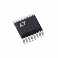
LT1568CGN Linear Technology, LT1568CGN Datasheet - Page 2

LT1568CGN
Manufacturer Part Number
LT1568CGN
Description
IC FILTER BUILDING BLOCK 16SSOP
Manufacturer
Linear Technology
Datasheet
1.LT1568CGNPBF.pdf
(16 pages)
Specifications of LT1568CGN
Filter Type
Bandpass
Frequency - Cutoff Or Center
200kHz
Number Of Filters
2
Max-order
2nd
Voltage - Supply
2.7 V ~ 11 V, ±2.7 V ~ 5.5 V
Mounting Type
Surface Mount
Package / Case
16-SSOP
Lead Free Status / RoHS Status
Contains lead / RoHS non-compliant
Available stocks
Company
Part Number
Manufacturer
Quantity
Price
Company:
Part Number:
LT1568CGN
Manufacturer:
LT
Quantity:
10 000
Part Number:
LT1568CGN
Manufacturer:
LINEAR/凌特
Quantity:
20 000
Company:
Part Number:
LT1568CGN#PBF
Manufacturer:
Diodes
Quantity:
9 106
Part Number:
LT1568CGN#PBF
Manufacturer:
LINEAR/凌特
Quantity:
20 000
ELECTRICAL CHARACTERISTICS
ABSOLUTE AXI U RATI GS
LT1568
(Note 1)
Total Supply Voltage (V
Input Voltage on INVA, INVB, GNDA and
GNDB Pins ....................................................... V
Input Current on INVA, INVB, GNDA and
GNDB Pins (Note 2) ........................................... 10mA
Output Short-Circuit Duration on OUTA, OUTB, OUTA
and OUTB Pins ............................................... Indefinite
Maximum Continuous Output Current (Note 3)
Specified Temperature Range (Note 9)
Junction Temperature .......................................... 150 C
Storage Temperature Range ................ – 65 C to 150 C
Lead Temperature (Soldering, 10 sec)................. 300 C
temperature range, otherwise specifications and typical values are at T
connected to midsupply, R
SYMBOL
V
I
I
2
S
OUT
S
DC ............................................................... 100mA
LT1568C ............................................ – 40 C to 85 C
LT1568I ............................................. – 40 C to 85 C
PARAMETER
Total Supply Voltage
Supply Current
Shutdown Supply Current
Output Voltage Swing High
(OUTA, OUTA, OUTB, OUTB Pins)
Output Voltage Swing Low
(OUTA, OUTA, OUTB, OUTB Pins)
Maximum Output Current
Op Amp Input Offset Voltage
Inverter Output Offset Voltage
W
FIL
+
to V
= R11 = R21 = R31 = R12 = R22 = R32, unless otherwise noted (see Block Diagram).
W W
–
) ........................... 11.6V
U
CONDITIONS
V
V
V
V
V
V
V
V
V
V
V
V
V
V
V
V
V
V
V
V
S
S
S
S
S
S
S
S
S
S
S
S
S
S
S
S
S
S
S
S
= 3V
= 5V
= 5V
= 3V, V
= 5V, V
= 5V, V
= 3V, R
= 5V, R
= 5V, R
= 5V, R
= 3V, R
= 5V, R
= 5V, R
= 5V, R
= 3V
= 5V
= 5V
= 3V
= 5V
= 5V
+
The
to V
EN
EN
FIL
FIL
FIL
FIL
FIL
FIL
EN
FIL
FIL
= 2.4V
= 4.4V
= 1.28k, R
= 1.28k, R
= 128 , R
= 1.28k, R
= 1.28k, R
= 128 , R
–
= 4.4V
= 1.28k, R
= 1.28k, R
denotes the specifications which apply over the full operating
PACKAGE/ORDER I FOR ATIO
Consult LTC Marketing for parts specified with wider operating temperature ranges.
A
L
L
L
L
L
L
= 25 C. V
L
L
= 1k
= 1k
= 1k
= 1k
= 400
= 400
= 1k
= 1k
GNDA
OUTA
OUTA
INVA
SA
NC
V
V
+
–
T
JMAX
S
16-LEAD PLASTIC SSOP
1
2
3
4
5
6
7
8
= single 5V, EN pin to logic “low,” R
= 150 C,
GN PACKAGE
TOP VIEW
JA
= 135 C/W
16
15
14
13
12
11
10
9
2.75
4.60
4.50
4.60
MIN
2.7
V
INVB
SB
OUTB
OUTB
GNDB
EN
V
–2.5
–2.5
–2.0
–10
–12
–2
+
–
U
2.85
4.80
4.65
4.75
0.05
0.07
0.20
TYP
0.3
0.5
1.0
24
26
28
–0.5
–4.0
80
0.2
1.2
2.5
0.6
ORDER PART
W
LT1568CGN
LT1568IGN
MARKING
GN PART
NUMBER
MAX
–4.7
0.12
0.15
0.40
1.0
1.3
2.5
11
35
36
38
1568
1568I
L
1.5
2.5
4.5
7.0
4.5
2.0
= 400 ,
UNITS
U
1568f
mA
mA
mA
mA
mA
mA
mA
mV
mV
mV
mV
mV
mV
V
V
V
V
V
V
V
V
V


