MJB5742T4G ON Semiconductor, MJB5742T4G Datasheet

TRANS PWR BIP NPN D2PAK

MJB5742T4G

Manufacturer Part Number
MJB5742T4G
Description
TRANS PWR BIP NPN D2PAK
Manufacturer
ON Semiconductor
Series
-r
Datasheet

Specifications of MJB5742T4G

Transistor Type
NPN - Darlington
Current - Collector (ic) (max)
8A
Voltage - Collector Emitter Breakdown (max)
400V
Vce Saturation (max) @ Ib, Ic
3V @ 400mA, 8A
Current - Collector Cutoff (max)
-
Dc Current Gain (hfe) (min) @ Ic, Vce
200 @ 4A, 5V
Power - Max
2W
Frequency - Transition
-
Mounting Type
*
Package / Case
*
Rohs Compliant
YES
Transistor Polarity
NPN
Power Dissipation Pd
2W
Dc Collector Current
8A
Dc Current Gain Hfe
200
Operating Temperature Range
-65°C To +150°C
Transistor Case Style
TO-263
No. Of Pins
3
Lead Free Status / Rohs Status
Lead free / RoHS Compliant

Available stocks

Company
Part Number
Manufacturer
Quantity
Price
Part Number:
MJB5742T4G
Manufacturer:
ON Semiconductor
Quantity:
500
MJB5742T4G
NPN Silicon Power
Darlington Transistors
switching in inductive circuits.
Features
Applications
Stresses exceeding Maximum Ratings may damage the device. Maximum
Ratings are stress ratings only. Functional operation above the Recommended
Operating Conditions is not implied. Extended exposure to stresses above the
Recommended Operating Conditions may affect device reliability.
1. Pulse Test: Pulse Width = 5 ms, Duty Cycle ≤ 10%.
MAXIMUM RATINGS
THERMAL CHARACTERISTICS
© Semiconductor Components Industries, LLC, 2011
June, 2011 − Rev. 2
Collector−Emitter Voltage
Emitter−Base Voltage
Collector Current
Base Current
Total Device Dissipation @ T
Derate above 25°C
Total Device Dissipation @ T
Derate above 25°C
Operating and Storage Junction
Temperature Range
Thermal Resistance, Junction−to−Case
Thermal Resistance, Junction−to−Ambient
Maximum Lead Temperature for Soldering
Purposes 1/8″ from Case for 5 Seconds
The Darlington transistors are designed for high−voltage power
These Devices are Pb−Free and are RoHS Compliant
Small Engine Ignition
Switching Regulators
Inverters
Solenoid and Relay Drivers
Motor Controls
Characteristics
Rating
− Continuous
− Peak (Note 1)
− Continuous
− Peak (Note 1)
A
C
= 25_C
= 25_C
V
Symbol
Symbol
T
CEO(sus)
V
R
R
J
V
I
I
P
P
, T
T
CEV
CM
BM
I
I
qJC
qJA
EB
C
B
D
D
L
stg
−65 to +150
Value
0.016
Max
1.25
62.5
400
800
100
275
2.5
0.8
16
8
8
5
2
1
W/_C
W/_C
_C/W
_C/W
Unit
Unit
Vdc
Vdc
Vdc
Adc
Adc
_C
_C
W
W
MJB5742T4G
†For information on tape and reel specifications,
including part orientation and tape sizes, please
refer to our Tape and Reel Packaging Specifications
Brochure, BRD8011/D.
Device
8 AMPERES, 400 VOLTS
POWER DARLINGTON
B5742
A
Y
WW
G
ORDERING INFORMATION
TRANSISTORS
http://onsemi.com
BASE
100 WATTS
1
≈ 100
= Specific Device Code
= Assembly Location
= Year
= Work Week
= Pb−Free Package
(Pb−Free)
Package
COLLECTOR 2,4
CASE 418B
D
STYLE 1
2
D
PAK
2
EMITTER 3
PAK
Publication Order Number:
≈ 50
800 / Tape & Reel
Shipping
MARKING
DIAGRAM
MJB5742/D
B5742G
AYWW

Related parts for MJB5742T4G

MJB5742T4G Summary of contents

Page 1

... R 62.5 _C/W qJA T 275 _C L MJB5742T4G †For information on tape and reel specifications, including part orientation and tape sizes, please refer to our Tape and Reel Packaging Specifications Brochure, BRD8011/D. 1 http://onsemi.com POWER DARLINGTON TRANSISTORS 8 AMPERES, 400 VOLTS 100 WATTS ≈ ...

Page 2

ELECTRICAL CHARACTERISTICS Î Î Î Î Î ...

Page 3

SECOND BREAKDOWN DERATING 80 60 THERMAL DERATING 100 T , CASE TEMPERATURE (°C) C Figure 1. Power Derating 2000 150°C 1000 25°C - 55°C 100 ...

Page 4

Table 1. Test Conditions for Dynamic Performance REVERSE BIAS SAFE OPERATING AREA AND INDUCTIVE SWITCHING 1N493 0.001 2N222 W 1 DUTY CYCLE ≤ 10 ≤ ...

Page 5

FORWARD BIAS There are two limitations on the power handling ability of a transistor: average junction temperature and second breakdown. Safe operating area curves indicate I limits of the transistor that must be observed for reliable operation; i.e., the transistor ...

Page 6

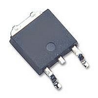
... −T− SEATING PLANE 0.13 (0.005 VARIABLE CONFIGURATION ZONE VIEW W−W 1 *For additional information on our Pb−Free strategy and soldering details, please download the ON Semiconductor Soldering and Mounting Techniques Reference Manual, SOLDERRM/D. PACKAGE DIMENSIONS 2 D PAK 3 CASE 418B−04 ISSUE VIEW W− ...

Page 7

... Opportunity/Affirmative Action Employer. This literature is subject to all applicable copyright laws and is not for resale in any manner. PUBLICATION ORDERING INFORMATION LITERATURE FULFILLMENT: Literature Distribution Center for ON Semiconductor P.O. Box 5163, Denver, Colorado 80217 USA Phone: 303−675−2175 or 800−344−3860 Toll Free USA/Canada Fax: 303− ...

Related keywords