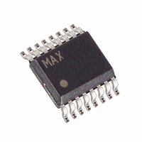
MAX7320AEE+T Maxim Integrated Products, MAX7320AEE+T Datasheet - Page 11

MAX7320AEE+T
Manufacturer Part Number
MAX7320AEE+T
Description
IC I/O EXPANDER I2C 8B 16QSOP
Manufacturer
Maxim Integrated Products
Datasheet
1.MAX7320ATE.pdf
(14 pages)
Specifications of MAX7320AEE+T
Interface
I²C
Number Of I /o
8
Interrupt Output
No
Frequency - Clock
400kHz
Voltage - Supply
1.71 V ~ 5.5 V
Operating Temperature
-40°C ~ 125°C
Mounting Type
Surface Mount
Package / Case
16-QSOP
Includes
POR
Lead Free Status / RoHS Status
Lead free / RoHS Compliant
SDA, SCL, AD0, AD2, and RST are overvoltage protect-
ed to +6V independent of V+. This allows the MAX7320
to be operated from a lower supply voltage, such as
+3.3V, while the I
logic level, such as +5V.
Each of the output ports, O0–O7, has a protection
diode to V+ and to GND (Figure 8). When a port output
is driven to a voltage higher than V+ or lower than
GND, the appropriate protection diode clamps the out-
put to a diode drop above V+ or below GND. When the
MAX7320 is powered down (V+ = 0V), each output port
appears as a diode connected to GND (Figure 8).
The MAX7320 operates with a supply voltage of +1.71V
to +5.5V over the -40°C to +125°C temperature range.
Bypass V+ to GND with a ceramic capacitor of at least
0.047µF as close to the device as possible. For the TQFN
version, additionally connect the exposed pad to GND.
I
2
C Port Expander with Eight Push-Pull Outputs
Applications Information
Power-Supply Considerations
2
______________________________________________________________________________________
C interface is driven from a higher
SDA
SCL
RST
AD0
AD2
Hot Insertion
INPUT
FILTER
ON RESET
POWER-
CONTROL
I
2
C
GND
V+
Figure 8. Output Port Structure
MAX7320
OUTPUT
MAX7320
PORTS
Functional Block Diagram
O6
O0
O7
O5
O4
O3
O2
O1
V+
V+
PORT
11


