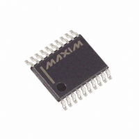
DS4550E+T&R Maxim Integrated Products, DS4550E+T&R Datasheet - Page 8

DS4550E+T&R
Manufacturer Part Number
DS4550E+T&R
Description
IC I/O EXPANDER I2C 9B 20TSSOP
Manufacturer
Maxim Integrated Products
Datasheet
1.DS4550ETR.pdf
(18 pages)
Specifications of DS4550E+T&R
Interface
I²C
Number Of I /o
9
Interrupt Output
No
Frequency - Clock
400kHz
Voltage - Supply
2.7 V ~ 5.5 V
Operating Temperature
-40°C ~ 85°C
Mounting Type
Surface Mount
Package / Case
20-TSSOP
Includes
EEPROM, JTAG
Lead Free Status / RoHS Status
Lead free / RoHS Compliant
The DS4550 memory map is shown in
different types of memory are present in the DS4550:
EEPROM, SRAM-shadowed EEPROM, and SRAM.
Memory locations specified as EEPROM are NV.
Writing to these locations results in an EEPROM write
cycle for a time specified by t
Characteristics table. Locations specified as SRAM-
shadowed EEPROM can be configured to operate in
one of two modes specified by the SEE bit (the LSB of
the Configuration Register, F4h). When the SEE bit = 0
I
Expander Plus Memory
Table
8
00h to 3Fh
40 to E7h
E8 to EFh
F0h
F1h
F2h
F3h
F4h
F5h to F7h
F8h
F9h
FAh to FFh
2
ADDRESS
C and JTAG Nonvolatile 9-Bit I/O
_____________________________________________________________________
1. DS4550 Memory Map
Memory Map and Memory Types
EEPROM
EEPROM
SRAM
Shadowed
EEPROM
[EEPROM
writes are
disabled if
the SEE bit
= 1]
SRAM
TYPE
User Memory
Reserved
Reserved
Pullup Enable
0
Pullup Enable
1
I/O Control 0
I/O Control 1
Configuration
User Memory
I/O Status 0
I/O Status 1
SRAM User
Memory
NAME
WR
in the AC Electrical
Table
64 Bytes of General-Purpose User EEPROM.
Undefined Address Space for Future Expansion. Reads and writes to
this space will have no affect on the device.
Pullup Enable for I/O_0 to I/O_7. I/O_0 is the LSB and I/O_7 is the
MSB. Set the corresponding bit to enable the pullup; clear the bit to
disable the pullup.
Pullup Enable for I/O_8. I/O_8 is the LSB. Only the LSB is used. Set
the LSB bit to enable the pullup on I/O_8; clear the LSB to disable the
pullup.
I/O Control for I/O_0 to I/O_7. I/O_0 is the LSB and I/O_7 is the MSB.
Clearing the corresponding bit of the register pulls the selected I/O
pin low; setting the bit places the pulldown transistor into a high-
impedance state. When the pulldown is high impedance, the output
will float if no pullup/down is connected to the pin.
I/O Control for I/O_8. I/O_8 is the LSB. Only the LSB is used. Clearing
the LSB of the register pulls the I/O_8 pin low; setting the LSB will
place the pulldown transistor into a high-impedance state. When the
pulldown is high impedance, the output will float if no pullup/down is
connected to the pin.
Configuration Register. The LSB is the SEE bit. When set, this bit
disables writes to the EEPROM; writing only effects the shadow
SRAM. When set to 0, both the EEPROM and the shadow SRAM is
written
3 bytes of General-Purpose User EEPROM
I/O Status for I/O_0 to I/O_7. I/O_0 is the LSB and I/O_7 is the MSB.
Writing to this register has no effect. Read this register to determine
the state of the I/O_0 to I/O_7 pins.
I/O Status for I/O_8. I/O_8 is the LSB. Only the LSB is used; the other
bits could be any value when read. Writing to this register has no
effect. Read this register to determine the state of the I/O_8 pin.
6 Bytes of General-Purpose SRAM
1. Three
(default), the memory location acts like EEPROM.
However, when SEE = 1, shadow SRAM is written to
instead of the EEPROM. This eliminates both the EEP-
ROM write time, t
out the EEPROM. This is ideal for applications that wish
to constantly write to the I/Os. Power-up default states
can be programmed for the I/Os in EEPROM (with SEE
= 0) and then once powered up, SEE can be written to
a 1 so that the I/Os can be updated periodically in
SRAM. The final type of memory present in the DS4550
is standard SRAM.
FUNCTION
WR
, as well as the concern of wearing
FACTORY
DEFAULT
00h
00h
00h
FFh
01h
00h
00h


