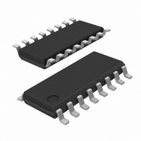
SI3056-D-FS Silicon Laboratories Inc, SI3056-D-FS Datasheet - Page 82

SI3056-D-FS
Manufacturer Part Number
SI3056-D-FS
Description
IC ISOMODEM SYSTEM-SIDE 16SOIC
Manufacturer
Silicon Laboratories Inc
Type
Chipsetr
Datasheet
1.SI3056-D-FS.pdf
(94 pages)
Specifications of SI3056-D-FS
Package / Case
16-SOIC (3.9mm Width)
Data Format
V.92
Interface
Serial
Voltage - Supply
3 V ~ 3.6 V
Mounting Type
Surface Mount
Product
Modem Module
Supply Voltage (min)
3 V
Supply Current
15 mA
Maximum Operating Temperature
+ 70 C
Minimum Operating Temperature
0 C
Mounting Style
SMD/SMT
Lead Free Status / RoHS Status
Lead free / RoHS Compliant
Baud Rates
-
Lead Free Status / RoHS Status
Lead free / RoHS Compliant, Lead free / RoHS Compliant
Available stocks
Company
Part Number
Manufacturer
Quantity
Price
Company:
Part Number:
SI3056-D-FS
Manufacturer:
FAIRCHILD
Quantity:
130
Company:
Part Number:
SI3056-D-FSR
Manufacturer:
DSC
Quantity:
1 200
Si3018/19/10
Register 59. Spark Quenching Control
Reset settings = 0000_0000
82
Name
Bit
Type
7
6
5
4
3
2
1
0
Bit
Reserved Always write this bit to zero.
Reserved Always write this bit to zero.
Reserved Always write this bit to zero.
Name
GCE
SQ1
SQ0
RG1
TB3
R/W
TB3
D7
For South Korea PTT compliance, set this bit, in addition to the RZ bit, to synthesize a ringer
impedance to meet South Korea ringer impedance requirements. This bit should only be set
to meet South Korea PTT requirements and should only be set in conjunction with the RZ bit.
Spark Quenching.
This bit, in combination with the OHS bit (Register 16), and the OHS2 bit (Register 31), sets
the amount of time for the line-side device to go on-hook. The on-hook speeds specified are
measured from the time the OH bit is cleared until loop current equals zero.
OHS
Spark Quenching.
This bit, in combination with the OHS bit (Register 16), and the OHS2 bit (Register 31), sets
the amount of time for the line-side device to go on-hook. The on-hook speeds specified are
measured from the time the OH bit is cleared until loop current equals zero.
OHS
Receive Gain 1 (Line-side Revision E or later).
This bit enables receive path gain adjustment.
0 = No gain applied to hybrid, full scale RX on line = 0 dBm.
1 = 1 dB of gain applied to hybrid, full scale RX on line = –1 dBm.
Guarded Clear Enable (Line-side Revision E or later).
This bit (in conjunction with the RZ bit set to 1), enables the Si3056 to meet BT’s Guarded
Clear Spec (B5 6450, Part 1: 1993, Section 15.4.3.3). With these bits set, the DAA will draw
approximately 2.5 mA of current from the line while on-hook.
0 = default, DAA does not draw loop current.
1 = Guarded Clear enabled, DAA draws 2.5 mA while on-hook to meet Guarded Clear
requirement.
SQ1
R/W
0
0
1
0
0
1
D6
OHS2
OHS2
D5
0
1
X
0
1
X
SQ0
R/W
D4
SQ[1:0]
SQ[1:0]
00
00
11
00
00
11
D3
Rev. 1.05
RG1
R/W
D2
Function
Less than 0.5 ms
3 ms ±10% (meets ETSI standard)
26 ms ±10% (meets Australia spark quenching
spec)
Less than 0.5 ms
3 ms ±10% (meets ETSI standard)
26 ms ±10% (meets Australia spark quenching
spec)
Mean On-Hook Speed
Mean On-Hook Speed
GCE
R/W
D1
D0


