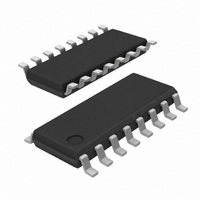
SI2493-C-FS Silicon Laboratories Inc, SI2493-C-FS Datasheet - Page 155

SI2493-C-FS
Manufacturer Part Number
SI2493-C-FS
Description
IC ISOMODEM SYSTEM-SIDE 16SOIC
Manufacturer
Silicon Laboratories Inc
Specifications of SI2493-C-FS
Mfg Application Notes
SI2493/57/34/15/04, Appl Note AN93
Data Format
V.21, V.22, V.23, V.29, V.32, V.34, V.90, V.92, Bell 103, Bell 212A
Baud Rates
56k
Interface
UART
Voltage - Supply
3 V ~ 3.6 V
Mounting Type
Surface Mount
Package / Case
16-SOIC (3.9mm Width)
Lead Free Status / RoHS Status
Lead free / RoHS Compliant
Available stocks
Company
Part Number
Manufacturer
Quantity
Price
Company:
Part Number:
SI2493-C-FSR
Manufacturer:
DY
Quantity:
8 623
Part Number:
SI2493-C-FSR
Manufacturer:
SIEMENS/西门子
Quantity:
20 000
- Current page: 155 of 230
- Download datasheet (7Mb)
P
15
16
17
18
19
20
21
22
23
24
25
26
27
28
29
30
31
#
The traces from the RJ11 through R7 and R8 to U2 pin 8 and pin 9 should be well
matched. These traces may be up to 10 cm long.
Distance from TIP and RING through EMC capacitors C8 and C9 to chassis ground is
short.
There should be no digital ground plane in the DAA Section.
Minimize the area of the loop from U2 pin 7 and pin 10 to C5 and C6 and from those
components to U2 pin 15 (IGND).
R2 should be placed next to the base of Q5, and the trace from R2 to U2 pin16 should be
less than 20 mm.
Place C4 close to U2 and connect C4 to U2 using a short, direct trace.
The area of the loop formed from U2 pin 13 to the base of Q4 and from U2 pin 12 to the
emitter of Q4 should be minimized.
The trace from C7 to U2 pin 15 should be short and direct.
The trace from C3 to the D1/D2 node should be short and direct.
Provide a minimum of 5 mm creepage (or use the capacitor terminal plating spacing as a
guideline for small form factor applications) from any TNV component, pad or trace, to
any SELV component, pad or trace.
Minimize the area of the loop formed from U2 pin 4 to R9 to U2 pin 15.
Cathode marking for Z1.
Pin 1 marking for U1 and U2.
Space and mounting holes to accommodate for fire enclosure if necessary.
IGND plane does not extend under C3, D1, FB1, FB2, R15, R16, C8, C9, or RV1.
Size Q3, Q4, and Q5 collector pads to safely dissipate 0.5 W (see text).
Submit layout to Silicon Laboratories for review.
Table 101. Layout Check List (Continued)
Layout Items
Rev. 0.9
AN93
Required
155
Related parts for SI2493-C-FS
Image
Part Number
Description
Manufacturer
Datasheet
Request
R
Part Number:
Description:
SOIC 16/C�/56 KBPS, V.92 ISOMODEM 16-PIN SYSTEM-SIDE - LEAD-FREE
Manufacturer:
Silicon Laboratories Inc
Part Number:
Description:
TSSOP 24/I�/56 KBPS, V.92 ISOMODEM SYSTEM-SIDE
Manufacturer:
Silicon Laboratories Inc
Part Number:
Description:
IC ISOMODEM SYSTEM-SIDE 24TSSOP
Manufacturer:
Silicon Laboratories Inc
Datasheet:
Part Number:
Description:
56 KBPS, V.92 ISOMODEM SYSTEM-SIDE - LEAD-FREE TSSOP 0 TO 7
Manufacturer:
Silicon Laboratories Inc
Datasheet:
Part Number:
Description:
Telecom ICs CONTACT SILICON LABS FOR AVAILABILITY
Manufacturer:
Silicon Laboratories Inc
Part Number:
Description:
IC ISOMODEM SYSTEM-SIDE 16SOIC
Manufacturer:
Silicon Laboratories Inc
Datasheet:
Part Number:
Description:
IC ISOMODEM SYSTEM-SIDE 24TSSOP
Manufacturer:
Silicon Laboratories Inc
Datasheet:

Part Number:
Description:
IC ISOMODEM W/ERROR CORR 16SOIC
Manufacturer:
Silicon Laboratories Inc
Datasheet:
Part Number:
Description:
IC ISOMODEM W/ERROR CORR 24TSSOP
Manufacturer:
Silicon Laboratories Inc
Datasheet:

Part Number:
Description:
IC ISOMODEM W/DAA 16SOIC
Manufacturer:
Silicon Laboratories Inc
Datasheet:
Part Number:
Description:
IC ISOMODEM SYSTEM-SIDE 24TSSOP
Manufacturer:
Silicon Laboratories Inc
Datasheet:
Part Number:
Description:
IC ISOMODEM W/ERROR CORR 24TSSOP
Manufacturer:
Silicon Laboratories Inc
Datasheet:
Part Number:
Description:
IC ISOMODEM W/DAA 24TSSOP
Manufacturer:
Silicon Laboratories Inc
Datasheet:


