MXB7843EEE+ Maxim Integrated Products, MXB7843EEE+ Datasheet - Page 16

MXB7843EEE+
Manufacturer Part Number
MXB7843EEE+
Description
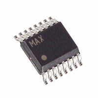
IC CNTRLR TOUCH RES 16QSOP
Manufacturer
Maxim Integrated Products
Type
Resistiver
Datasheet
1.MXB7843EEE.pdf
(21 pages)
Specifications of MXB7843EEE+
Touch Panel Interface
4-Wire
Number Of Inputs/keys
1 TSC
Resolution (bits)
12 b
Data Interface
MICROWIRE™, QSPI™, Serial, SPI™
Data Rate/sampling Rate (sps, Bps)
125k
Voltage Reference
External
Voltage - Supply
2.38 V ~ 5.25 V
Current - Supply
650µA
Operating Temperature
-40°C ~ 85°C
Mounting Type
Surface Mount
Package / Case
16-QSOP
Output Type
Digital
Interface
4-Wire Serial
Input Type
Analog
Maximum Operating Temperature
+ 85 C
Mounting Style
SMD/SMT
Minimum Operating Temperature
- 40 C
Lead Free Status / RoHS Status
Lead free / RoHS Compliant
pointing device presses on the touch screen, the Y+
and Y- drivers are turned on, connecting one side of
the vertical resistive layer to V
ground. In this case, the horizontal resistive layer func-
tions as a sense line. One side of this resistive layer
gets connected to the X+ input, while the other side is
left open or floating. The point where the touch screen
is pressed brings the two resistive layers in contact and
forms a voltage-divider at that point. The data converter
senses the voltage at the point of contact through the
X+ input and digitizes it. The horizontal layer resistance
does not introduce any error in the conversion because
no DC current is drawn.
The conversion process of the analog input voltage to
digital output is controlled through the serial interface
between the A/D converter and the µP. The processor
controls the MXB7843 configuration through a control
byte (Tables 3 and 4). Once the processor instructs the
MXB7843 to initiate a conversion, the MXB7843 biases
the touch screen through the internal switches at the
beginning of the acquisition period. The voltage transient
at the touch screen needs to settle down to a stable volt-
age before the acquisition period is over. After the acqui-
sition period is over, the A/D converter goes into a
conversion period with all internal switches turned off if
the device is in single-ended mode. If the device is in
differential mode, the internal switches remain on from
the start of the acquisition period to the end of the con-
version period.
When power is first applied, internal power-on circuitry
resets the MXB7843. Allow 10µs for the first conversion
after the power supplies stabilize. If CS is low, the first
logic 1 on DIN is interpreted as a start bit. Until a con-
version takes place, DOUT shifts out zeros.
Save power by placing the converter in one of two low-
current operating modes or in full power-down between
conversions. Select the power-down mode through
PD1 and PD0 of the control byte (Tables 3 and 4).
The software power-down modes take effect after the
conversion is completed. The serial interface remains
active while waiting for a new control byte to start a con-
version and switches to full-power mode. After complet-
ing its conversion, the MXB7843 enters the programmed
power mode until a new control byte is received.
The power-up wait before conversion period is depen-
dent on the power-down state. When exiting software
low-power modes, conversion can start immediately
when running at decreased clock rates. Upon power-
on reset, the MXB7843 is in power-down mode with
2.375V to 5.25V, 4-Wire Touch-Screen
Controller
16
______________________________________________________________________________________
DD
and the other side to
Power-On Reset
Power Modes
PD1 = 0 and PD0 = 0. When exiting software shutdown,
the MXB7843 is ready to perform a conversion in 10µs.
In this mode, the MXB7843 is always powered. The
device remains fully powered after the current conver-
sion completes.
In this mode, the MXB7843 powers down after the current
conversion completes or on the next rising edge of CS,
whichever occurs first. The next control byte received on
DIN powers up the MXB7843. At the start of a new con-
version, it instantly powers up. When each conversion is
finished, the part enters power-down mode, unless other-
wise indicated. The first conversion after the ADC returns
to full power is valid for differential conversions and sin-
gle-ended measurement conversions.
When operating at full speed and 16 clocks per conver-
sion, the difference in power consumption between
PD1 = 0, PD0 = 1, and PD1 = 0, PD0 = 0 is negligible.
Also, in the case where the conversion rate is
decreased by slowing the frequency of the DCLK input,
the power consumption between these two modes is
not very different. When the DCLK frequency is kept at
Figure 10. Ideal Input Voltages and Output Codes
11…111
11…110
11…101
00…011
00…010
00…001
00…000
OUTPUT CODE
0
1
2
3
INPUT VOLTAGE (LSB) = [(V
FULL-SCALE
TRANSITION
+IN
) - (V
FS-3/2LSB
-IN
PD1 = 1, PD0 = 1
PD1 = 0, PD0 = 0
)]
1LSB =
FS = (V
FS
(V
REF+
REF+
4096
- V
- V
REF-
REF-
)
)


