AD2S80AJD Analog Devices Inc, AD2S80AJD Datasheet - Page 4
AD2S80AJD
Manufacturer Part Number
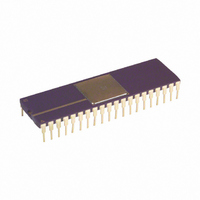
AD2S80AJD
Description
IC R/D CONV TRACKING 40CDIP
Manufacturer
Analog Devices Inc
Type
R/D Converterr
Specifications of AD2S80AJD
Rohs Status
RoHS non-compliant
Input Type
Parallel
Output Type
Digital
Interface
Parallel
Current - Supply
30mA
Mounting Type
Through Hole
Package / Case
40-CDIP (0.600", 15.24mm)
Resolution (bits)
16bit
Input Channel Type
Differential
Data Interface
Parallel
Supply Voltage Range - Analog
± 10.8V To ± 13.2V
Supply Current
19mA
Digital Ic Case Style
DIP
No. Of Pins
40
Lead Free Status / RoHS Status
Contains lead / RoHS non-compliant
Available stocks
Company
Part Number
Manufacturer
Quantity
Price
Company:

Part Number:
AD2S80AJD
Manufacturer:
FUJI
Quantity:
3 000
Company:
Part Number:
AD2S80AJD
Manufacturer:
AD
Quantity:
5 510
Company:
Part Number:
AD2S80AJD
Manufacturer:
ADI
Quantity:
741
Part Number:
AD2S80AJD
Manufacturer:
ADI/亚德诺
Quantity:
20 000


CAUTION
ESD (electrostatic discharge) sensitive device. Electrostatic charges as high as 4000 V readily
accumulate on the human body and test equipment and can discharge without detection. Although
the AD2S80A features proprietary ESD protection circuitry, permanent damage may occur on
devices subjected to high-energy electrostatic discharges. Therefore, proper ESD precautions are
recommended to avoid performance degradation or loss of functionality.
AD2S80A–SPECIFICATIONS
Parameter
RATIO MULTIPLIER
PHASE SENSITIVE DETECTOR
INTEGRATOR
VCO
POWER SUPPLIES
Specification subject to change without notice.
All min and max specifications are guaranteed. Specifications in boldface are tested on all production units at final electrical test.
AC Error Output Scaling
Output Offset Voltage
Gain
Input Bias Current
Input Impedance
Input Voltage
Open-Loop Gain
Dead Zone Current (Hysteresis)
Input Offset Voltage
Input Bias Current
Output Voltage Range
Maximum Rate
VCO Rate
VCO Power Supply Sensitivity
Input Offset Voltage
Input Bias Current
Input Bias Current Tempco
Input Voltage Range
Linearity of Absolute Rate
Reversion Error
Sensitivity of Reversion Error
Voltage Levels
Current
In Phase
In Quadrature
Increase
Decrease
Full Range
Over 0% to 50% of Full Range
to Symmetry of Power Supplies
+V
–V
+V
± I
± I
± I
S
S
L
S
S
L
Conditions
10 Bit
12 Bit
14 Bit
16 Bit
w.r.t. REF
w.r.t. REF
At 10 kHz
± V
± V
Positive Direction
Negative Direction
+V
–V
+V
–V
± V
± V
+V
S
S
S
S
S
S
S
S
L
= ± 10.8 V dc
= ± 12 V dc
@ ± 12 V
@ 13.2 V
@ ± 5.0 V
(typical at 25 C unless otherwise noted)
Min
–0.882
1
57
± 7
7.1
7.1
+10.8
–10.8
+5
Typ
177.6
44.4
11.1
2.775
–0.9
60
100
1
60
7.9
7.9
+0.5
–8.0
–8.0
+2.0
1
70
–1.22
± 8
12
19
0.5
WARNING!
Max
12
–0.918
± 0.02
150
± 8
63
5
150
1.1
8.7
8.7
5
380
± 8
<2
<1
1.5
+13.2
–13.2
+13.2
23
30
1.5
ESD SENSITIVE DEVICE
Unit
mV/Bit
mV/Bit
mV/Bit
mV/Bit
mV
V rms/V dc
V rms/V dc
nA
MΩ
V
dB
nA/LSB
mV
nA
V
MHz
kHz/µA
kHz/µA
%/V
%/V
%/V
%/V
mV
nA
nA/°C
V
% FSD
% FSD
% FSD
%/V of
Asymmetry
V
V
V
mA
mA
mA
Related parts for AD2S80AJD
Image
Part Number
Description
Manufacturer
Datasheet
Request
R

Part Number:
Description:
±1.7g Dual-Axis IMEMS Accelerometer Evaluation Board
Manufacturer:
Analog Devices Inc
Datasheet:

Part Number:
Description:
Inertial Sensor Evaluation System
Manufacturer:
Analog Devices Inc
Datasheet:
Part Number:
Description:
Manufacturer:
Analog Devices Inc
Datasheet:
Part Number:
Description:
Manufacturer:
Analog Devices Inc
Datasheet:
Part Number:
Description:
Manufacturer:
Analog Devices Inc
Datasheet:
Part Number:
Description:
Manufacturer:
Analog Devices Inc
Datasheet:
Part Number:
Description:
Manufacturer:
Analog Devices Inc
Datasheet:
Part Number:
Description:
Manufacturer:
Analog Devices Inc
Datasheet:
Part Number:
Description:
Manufacturer:
Analog Devices Inc
Datasheet:
Part Number:
Description:
Manufacturer:
Analog Devices Inc
Datasheet:
Part Number:
Description:
Manufacturer:
Analog Devices Inc
Datasheet:
Part Number:
Description:
Manufacturer:
Analog Devices Inc
Datasheet:
Part Number:
Description:
Manufacturer:
Analog Devices Inc
Datasheet: