QT60240-ISG Atmel, QT60240-ISG Datasheet - Page 10
QT60240-ISG
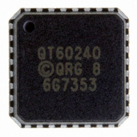
Manufacturer Part Number
QT60240-ISG
Description
SENSOR IC MTRX TOUCH24KEY 32-QFN
Manufacturer
Atmel
Series
QMatrix™r
Type
Capacitiver
Datasheet
1.QT60160-ISG.pdf
(26 pages)
Specifications of QT60240-ISG
Number Of Inputs/keys
24 Key
Resolution (bits)
10 b
Data Interface
I²C, Serial, SPI™
Voltage Reference
External
Voltage - Supply
1.8V, 3.3V, 5V
Current - Supply
4.6mA
Operating Temperature
-40°C ~ 85°C
Mounting Type
Surface Mount
Package / Case
32-MLF®, QFN
Output Type
*
Interface
*
Input Type
*
Operating Supply Voltage
1.8 V to 5.5 V
Maximum Operating Temperature
+ 85 C
Mounting Style
SMD/SMT
Minimum Operating Temperature
- 40 C
Lead Free Status / RoHS Status
Lead free / RoHS Compliant
Other names
427-1126-2
Available stocks
Company
Part Number
Manufacturer
Quantity
Price
Company:

Part Number:
QT60240-ISG
Manufacturer:
TAYIO
Quantity:
60 000


3 Interfaces
3.1 Introduction
The QT60xx0 can be configured to communicate either over
an I
(SPI).
The pins A0, A1 are used to configure the type of interface
and the I
addresses are available as shown in Table 3.1 below.
3.2 Shift Register Output Mode
When the option jumpers are both set at Vss, the device
disables the I
suitable for driving a shift register.
The shift register data is output at pin 27 (SDA). The clock is
output at pin 28 (SCL). The data is clocked on the
positive-going transition of SCL. Data is transferred from the
shift registers to the latched outputs on the positive-going
transition of LATCH. An example shift register connection is
shown in Figure 3.1.
The shift register data is output over the duration of a matrix
scan, as each key is being processed, and it is latched at the
end of the scan. The overall communication time depends on
the matrix scan time.
lQ
2
Parameter
SCL low pulse width
SCL high pulse width
LATCH pulse width
SDA data to SCL clock hold time
C bus or a shift register type Serial Peripheral Interface
2
C address if this mode is used. The modes and I
2
Vdd
Vdd
Vss
Vss
C interface and instead generates output
A1
Table 3.1 Interface Details
Table 3.2 Shift Register
Vdd
Vdd
Vss
Vss
A0
QT60160/60240
Shift Register
I
I
I
Latch
2
2
2
SDA
SCL
C Address 7
C Address 17
C Address 117
Legend
t
t
t
t
SCL
SCH
LATCH
SDA
Interface
-
28
SCL
27
9
Units
500ns min
125us min
500ns min
75us min
Figure 3.1 Shift Register Output
2
C
10
Figure 3.2, page 11 shows a full shift register cycle with keys
3, 10 and 15 activated. Key Scan represents the time when
the chip is measuring signal from each key. SCL, SDA and
LATCH represent their respective signals from the chip. SCL
is an active low clock output. SDA is the data output; high if
the key is in detect and low if it is not. LATCH pulses low
when the data transfer is complete.
Data output proceeds as soon as the key has been
processed. Most keys do not get processed during the key
scan. If so, these keys are processed and the data is output
after the complete key scan.
The internal settings of the device in Shift Register mode are
the default factory settings found in Table 6.2. This means the
device will operate with a Burst Length of 48 on all keys, and
a Sleep time of 125ms for example. These settings cannot be
changed in this mode.
In Shift Register mode, the CHANGE pin is inactive and
should be left open.
3.3 I
These devices use I
The QT60160/QT60240 will only respond to the correct
address match. I
The match address is selected via pins A0 and A1. Table 3.1
shows the address selections.
The QT60160/QT60240 allows multiple byte transmissions to
provide a more efficient communication. This is particularly
useful to retrieve several information bytes at once. Every
time the host retrieves data from the QT60160/QT60240, an
internal address pointer is incremented.
Therefore, the host only needs to write the initial address
pointer of interest (the lowest address), followed by read
cycles for as many bytes as required.
DS
SH_CP
ST_CP
DS
SH_CP
ST_CP
DS
SH_CP
ST_CP
74HC595
74HC595
74HC595
Max Data Transfer:
Address:
2
C Port
Q0
Q2
Q3
Q4
Q5
Q6
Q7
/Q7
Q0
Q2
Q3
Q4
Q5
Q6
Q7
/Q7
Q0
Q2
Q3
Q4
Q5
Q6
Q7
/Q7
2
C operating parameters are as follows:
Outputs, keys 16 to 23
Outputs, keys 8 to 15
Outputs, keys 0 to 7
2
C communications, in slave mode only.
QT60240-ISG R8.06/0906
100KHz
7-bit
Related parts for QT60240-ISG
Image
Part Number
Description
Manufacturer
Datasheet
Request
R

Part Number:
Description:
Microcontrollers (MCU) 1.8 - 5.5V 24 Chan QMatrix
Manufacturer:
Atmel

Part Number:
Description:
Interface - Specialized Integrated Circuit
Manufacturer:
Atmel
Datasheet:

Part Number:
Description:
DEV KIT FOR AVR/AVR32
Manufacturer:
Atmel
Datasheet:

Part Number:
Description:
INTERVAL AND WIPE/WASH WIPER CONTROL IC WITH DELAY
Manufacturer:
ATMEL Corporation
Datasheet:
Part Number:
Description:
Low-Voltage Voice-Switched IC for Hands-Free Operation
Manufacturer:
ATMEL Corporation
Datasheet:
Part Number:
Description:
MONOLITHIC INTEGRATED FEATUREPHONE CIRCUIT
Manufacturer:
ATMEL Corporation
Datasheet:
Part Number:
Description:
AM-FM Receiver IC U4255BM-M
Manufacturer:
ATMEL Corporation
Datasheet:
Part Number:
Description:
Monolithic Integrated Feature Phone Circuit
Manufacturer:
ATMEL Corporation
Datasheet:
Part Number:
Description:
Multistandard Video-IF and Quasi Parallel Sound Processing
Manufacturer:
ATMEL Corporation
Datasheet:
Part Number:
Description:
High-performance EE PLD
Manufacturer:
ATMEL Corporation
Datasheet:
Part Number:
Description:
8-bit Flash Microcontroller
Manufacturer:
ATMEL Corporation
Datasheet: