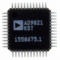
AD9821KSTZ Analog Devices Inc, AD9821KSTZ Datasheet - Page 13

AD9821KSTZ
Manufacturer Part Number
AD9821KSTZ
Description
IC IMAGE SGNL PROC 12BIT 48-LQFP
Manufacturer
Analog Devices Inc
Type
Image Sensorr
Datasheet
1.AD9821KST.pdf
(16 pages)
Specifications of AD9821KSTZ
Input Type
Logic
Output Type
Logic
Interface
3-Wire Serial
Mounting Type
Surface Mount
Package / Case
48-LQFP
Analog Front End Type
CCD
Analog Front End Category
Video
Interface Type
Serial (3-Wire)
Sample Rate
40MSPS
Input Voltage Range
0.5V
Operating Supply Voltage (min)
2.7V
Operating Supply Voltage (typ)
3.3V
Operating Supply Voltage (max)
3.6V
Resolution
12b
Number Of Adc's
1
Power Supply Type
Analog/Digital
Operating Temp Range
-20C to 85C
Operating Temperature Classification
Commercial
Mounting
Surface Mount
Pin Count
48
Package Type
LQFP
Number Of Channels
1
Lead Free Status / RoHS Status
Lead free / RoHS Compliant
Current - Supply
-
Lead Free Status / RoHS Status
Compliant, Lead free / RoHS Compliant
Available stocks
Company
Part Number
Manufacturer
Quantity
Price
APPLICATIONS INFORMATION
The AD9821 is a complete Analog Front End (AFE) product
for a variety of imager applications using CMOS image sensors
and CCDs with on-chip CDS. As shown in Figure 10, the imager
output is generally buffered and sent to the AD9821’s analog
inputs, either as a differential or single-ended signal. The AD9821
performs the sample-and-hold operation, gain adjustment,
black level correction, and analog-to-digital conversion. The
REV. 0
OUTPUTS
DATA
12
SUPPLY
DRIVER
IMAGER
(MSB) D11
CMOS
V-DRIVE
INTERFACE
CCD
(CCD)
OR
3V
SERIAL
D10
D0
D1
D2
D3
D4
D5
D6
D7
D8
D9
0.1 F
OUT+
OUT–
10
11
12
1
2
3
4
5
6
7
8
9
48 47 46 45 44
13 14 15 16 17 18 19 20 21 22 23 24
PIN 1
IDENTIFIER
3
Figure 13. Recommended Circuit Configuration
LEVEL SHIFT
ANALOG SUPPLY
0.1 F
BUFFER
Figure 12. System Applications Diagram
OR
(Not to Scale)
3V
AD9821
TOP VIEW
43 42 41 40
ANALOG SUPPLY
IMAGER
TIMING
3V
39 38
VIN+
VIN–
3
GENERATOR
–13–
AD9821
37
TIMING
0.1 F
1.0 F
1.0 F
CLOCK
INPUTS
REGISTER-
36
35
34
33
32
31
30
29
28
27
26
25
DATACLK/CLAMP
TIMING
AD9821’s digital output data is then processed by the image
processing ASIC. The internal registers of the AD9821—used
to control gain, offset level, and other functions—are
programmed by the ASIC or microprocessor through a 3-wire
serial digital interface. A system timing generator provides the
clock signals for both the imager and the AFE.
ADC
TEST
AVSS
TEST
AVDD2
BYP1
VIN-
VIN+
TEST
TEST
AVDD1
AVSS
AVSS
DATA
OUT
NC = INTERNALLY NOT CONNECTED
OUTPUTS
INTERFACE
DIGITAL
0.1 F
SERIAL
0.1 F
0.1 F
3V
ANALOG SUPPLY
3V
ANALOG SUPPLY
IMAGER INPUT, NEGATIVE/REFERENCE
IMAGER INPUT, POSITIVE
DIGITAL IMAGE
PROCESSING
INCLUDE TG)
(MAY ALSO
ASIC
AD9821


