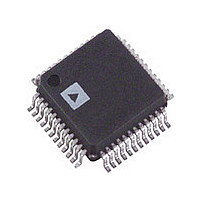
AD9841AJSTRL Analog Devices Inc, AD9841AJSTRL Datasheet

AD9841AJSTRL
Specifications of AD9841AJSTRL
Related parts for AD9841AJSTRL
AD9841AJSTRL Summary of contents
Page 1
PBLK CCDIN CLPDM AUX1IN AUX2IN CLP AD9841A/AD9842A PxGA is a registered trademark of Analog Devices, Inc. REV. 0 Information furnished by Analog Devices is believed to be accurate and reliable. However, no responsibility is assumed by Analog Devices for ...
Page 2
AD9841A/AD9842A–SPECIFICATIONS GENERAL SPECIFICATIONS Parameter TEMPERATURE RANGE Operating Storage POWER SUPPLY VOLTAGE Analog, Digital, Digital Driver POWER CONSUMPTION Normal Operation Power-Down Modes Fast Recovery Mode Standby Total Power-Down MAXIMUM CLOCK RATE A/D CONVERTER (AD9841A) Resolution Differential Nonlinearity (DNL) No Missing Codes ...
Page 3
AD9841A CCD-MODE SPECIFICATIONS Parameter P OWER CONSUMPTION MAXIMUM CLOCK RATE CDS Gain 1 Allowable CCD Reset Transient 1 Max Input Range Before Saturation 1 Max CCD Black Pixel Amplitude PIXEL GAIN AMPLIFIER (PxGA) Max Input Range Max Output Range Gain ...
Page 4
AD9841A/AD9842A–SPECIFICATIONS AD9842A CCD-MODE SPECIFICATIONS Parameter P OWER CONSUMPTION MAXIMUM CLOCK RATE CDS Gain 1 Allowable CCD Reset Transient 1 Max Input Range Before Saturation 1 Max CCD Black Pixel Amplitude PIXEL GAIN AMPLIFIER (PxGA) Max Input Range Max Output Range ...
Page 5
AUX1-MODE SPECIFICATIONS Parameter POWER CONSUMPTION MAXIMUM CLOCK RATE INPUT BUFFER Gain Max Input Range VGA Max Output Range Gain Control Resolution Gain (Selected Using VGA Gain Register) Min Gain Max Gain Specifications subject to change without notice. AUX2-MODE SPECIFICATIONS Parameter ...
Page 6
AD9841A/AD9842A (C TIMING SPECIFICATIONS Serial Timing in Figures 21–24.) Parameter SAMPLE CLOCKS DATACLK, SHP, SHD Clock Period DATACLK Hi/Low Pulsewidth SHP Pulsewidth SHD Pulsewidth CLPDM Pulsewidth 1 CLPOB Pulsewidth SHP Rising Edge to SHD Falling Edge SHP Rising Edge to ...
Page 7
NC 1 PIN IDENTIFIER 3 (LSB AD9841A D3 6 TOP VIEW 7 D4 (Not to Scale ...
Page 8
AD9841A/AD9842A DEFINITIONS OF SPECIFICATIONS DIFFERENTIAL NONLINEARITY (DNL) An ideal ADC exhibits code transitions that are exactly 1 LSB apart. DNL is the deviation from this ideal value. Thus every code must have a finite width. No missing codes guaranteed to ...
Page 9
Typical Performance Characteristics– 100 SAMPLE RATE – MHz 0.5 0.25 0 –0.25 –0.5 400 0 200 600 4 3 ...
Page 10
AD9841A/AD9842A CCD-MODE AND AUX MODE TIMING CCD SIGNAL SHP t S1 SHD t INH DATACLK t OD OUTPUT N–10 DATA NOTES: 1. RECOMMENDED PLACEMENT FOR DATACLK RISING EDGE IS BETWEEN THE SHD RISING EDGE AND ...
Page 11
PIXEL GAIN AMPLIFIER (PxGA) TIMING FRAME n VD 0101... 2323... LINE 0 LINE 1 HD NOTE GAIN0 GAIN1 GAIN2 GAIN3 5 PIXEL MIN VD HD SHP PxGA GAIN NOTES: 1. MINIMUM PULSEWIDTH ...
Page 12
AD9841A/AD9842A LINE n VD 012012012... HD NOTE GAIN0 GAIN1 GAIN2 5 PIXEL MIN VD 5 PIXEL MIN HD SHP PxGA GAIN NOTES: 1. BOTH VD AND HD ARE INTERNALLY UPDATED AT SHP RISING EDGES. ...
Page 13
VD EVEN FIELD 0101... 0101... 0101... LINE 0 LINE 1 LINE 2 HD NOTE GAIN0 GAIN1 GAIN2 GAIN3 VD 5 PIXEL MIN HD 3ns MIN SHP PxGA GAIN NOTES: 1. BOTH VD ...
Page 14
AD9841A/AD9842A VD HD 3ns MIN SHP GAIN0 PxGA GAIN NOTES: 1. BOTH VD AND HD ARE INTERNALLY UPDATED AT SHP RISING EDGES AND SELECTS GAIN0 AND ...
Page 15
SERIAL INTERFACE TIMING AND INTERNAL REGISTER DESCRIPTION Register Address Name Operation Channel Select Power-Down CCD/AUX1/2 Modes VGA Gain LSB Clamp Level LSB Control ...
Page 16
AD9841A/AD9842A 11 BITS OPERATION RNW ... SDATA ... SCK NOTES: 1. ANY NUMBER OF ADJACENT REGISTERS MAY BE LOADED SEQUENTIALLY, BEGINNING WITH THE LOWEST ...
Page 17
Table IV. AD9841A Clamp Level Register Contents (Default Value x080) MSB D10 Table V. AD9842A Clamp Level Register Contents (Default Value x080) MSB D10 ...
Page 18
AD9841A/AD9842A CIRCUIT DESCRIPTION AND OPERATION The AD9841A and AD9842A signal processing chain is shown in Figure 25. Each processing step is essential in achieving a high-quality image from the raw CCD pixel data. DC Restore To reduce the large dc ...
Page 19
MOSAIC SEPARATE COLOR CCD: PROGRESSIVE BAYER STEERING MODE LINE0 GAIN0, GAIN1, GAIN0, GAIN1 ... LINE1 GAIN2, GAIN3, GAIN2, GAIN3 ... LINE2 GAIN0, GAIN1, GAIN0, GAIN1 ... Gb B ...
Page 20
AD9841A/AD9842A A/D Converter The AD9841A and AD9842A use high-performance ADC archi- tectures, optimized for high speed and low power. Differential Nonlinearity (DNL) performance is typically better than 0.5 LSB, as shown in TPCs 2 and 4. Instead of the 1 ...
Page 21
APPLICATIONS INFORMATION The AD9841A and AD9842A are complete Analog Front End (AFE) products for digital still camera and camcorder appli- cations. As shown in Figure 32, the CCD image (pixel) data is buffered and sent to the AD984xA analog input ...
Page 22
AD9841A/AD9842A SERIAL INTERFACE (MSB) D11 12 DATA OUTPUTS 3V DRIVER SUPPLY Internal Power-On Reset Circuitry After power-on, the AD9842A will automatically reset all inter- nal registers and perform internal calibration procedures. This takes approximately complete. During this ...
Page 23
OUTLINE DIMENSIONS Dimensions shown in inches and (mm). 48-Lead LQFP (ST-48) 0.063 (1.60) MAX 0.354 (9.00) BSC SQ 0.030 (0.75 0.018 (0.45 TOP VIEW (PINS DOWN) COPLANARITY 12 25 0.003 (0.08 MIN 0.019 ...


