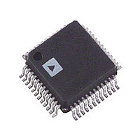
AD9844AJST Analog Devices Inc, AD9844AJST Datasheet

AD9844AJST
Specifications of AD9844AJST
Available stocks
Related parts for AD9844AJST
AD9844AJST Summary of contents
Page 1
PBLK CCDIN CLPDM AUX1IN AUX2IN CLP AD9844A PRODUCT DESCRIPTION The AD9844A is a complete analog signal processor for CCD applications. It features a 20 MHz single-channel architecture designed to sample and condition the outputs of interlaced and progressive scan ...
Page 2
AD9844A–SPECIFICATIONS GENERAL SPECIFICATIONS Parameter TEMPERATURE RANGE Operating Storage POWER SUPPLY VOLTAGE Analog, Digital, Digital Driver POWER CONSUMPTION Normal Operation Power-Down Modes Fast Recovery Mode Standby Total Power-Down MAXIMUM CLOCK RATE A/D CONVERTER Resolution Differential Nonlinearity (DNL) No Missing Codes Full-Scale ...
Page 3
CCD-MODE SPECIFICATIONS Parameter P OWER CONSUMPTION MAXIMUM CLOCK RATE CDS 1 Allowable CCD Reset Transient 1 Max CCD Black Pixel Amplitude 1 Max Input Range Before Saturation Max Input Range Before Saturation Max Input Range Before Saturation Max Output Range ...
Page 4
AD9844A–SPECIFICATIONS AUX1-MODE SPECIFICATIONS Parameter POWER CONSUMPTION MAXIMUM CLOCK RATE INPUT BUFFER Gain Max Input Range VGA Max Output Range Gain Control Resolution Gain (Selected Using VGA Gain Register) Min Gain Max Gain Specifications subject to change without notice. AUX2-MODE SPECIFICATIONS ...
Page 5
... SHP t 7 SHD t 4 CDM t 2 COB INH 7 SCLK Model Unit AD9844AJST –20°C to +85° THERMAL CHARACTERISTICS V Thermal Resistance V 48-Lead LQFP Package V θ = 92° °C 150 °C 300 AD9844A Typ Max Unit 12 Pixels 20 Pixels Cycles ...
Page 6
AD9844A CONNECT Pin Number Name 1–12 D0–D11 13 DRVDD 14 DRVSS 15, 18, 24, 41 DVSS 16 DATACLK 17 DVDD1 19 PBLK 20 CLPOB 21 SHP 22 SHD 23 CLPDM 25, 26, 35 AVSS 27 AVDD1 28 ...
Page 7
DEFINITIONS OF SPECIFICATIONS DIFFERENTIAL NONLINEARITY (DNL) An ideal ADC exhibits code transitions that are exactly 1 LSB apart. DNL is the deviation from this ideal value. Thus every code must have a finite width. No missing codes guaranteed to 12-bit ...
Page 8
Performance Characteristics AD9844A 100 SAMPLE RATE – MHz 0.5 0.25 0 –0.25 –0.5 0 500 1000 1500 2000 2500 ...
Page 9
CCD-MODE AND AUX-MODE TIMING CCD SIGNAL SHP t S1 SHD t INH DATACLK t OD OUTPUT N–10 DATA NOTES: 1. RECOMMENDED PLACEMENT FOR DATACLK RISING EDGE IS BETWEEN THE SHD RISING EDGE AND NEXT SHP ...
Page 10
AD9844A SERIAL INTERFACE TIMING AND INTERNAL REGISTER DESCRIPTION Register Address Name Operation Channel Select CCD/AUX VGA Gain LSB Clamp Level LSB Control CDS ...
Page 11
Table II. Operation Register Contents (Default Value x000) D10 Must be set to zero. Set to one. Table III. VGA Gain Register Contents (Default Value x096) MSB D10 ...
Page 12
AD9844A DC RESTORE 0.1 F CCDIN CLPDM CIRCUIT DESCRIPTION AND OPERATION The AD9844A signal processing chain is shown in Figure 11. Each processing step is essential in achieving a high-quality image from the raw CCD pixel data. DC Restore To ...
Page 13
Input Clamp A line-rate input clamping circuit is used to remove the CCD’s optical black offset. This offset exists in the CCD’s shielded black reference pixels. Unlike some AFE architectures, the AD9844A removes this offset in the input stage to ...
Page 14
AD9844A 0.8V ??V 0.1 F INPUT SIGNAL 0.4V AUX2IN VIDEO SIGNAL 0.1 F MSB D10 0.4V 0dB TO 36dB 5k AUX1IN VGA 10 0.4V VGA GAIN REGISTER ...
Page 15
CCD V OUT V-DRIVE APPLICATIONS INFORMATION The AD9844A is a complete Analog Front End (AFE) product for digital still camera and camcorder applications. As shown in Figure 16, the CCD image (pixel) data is buffered and sent to the AD9844A ...
Page 16
AD9844A SERIAL INTERFACE (MSB) D11 12 DATA OUTPUTS DRIVER SUPPLY 3V ANALOG SUPPLY 0.1 F 1 (LSB PIN 1 ...


