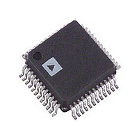
AD9849AKST Analog Devices Inc, AD9849AKST Datasheet - Page 23

AD9849AKST
Manufacturer Part Number
AD9849AKST
Description
IC CCD SIGNAL PROC 12BIT 48-LQFP
Manufacturer
Analog Devices Inc
Type
CCD Signal Processor, 12-Bitr
Datasheet
1.AD9849AKSTZRL.pdf
(32 pages)
Specifications of AD9849AKST
Rohs Status
RoHS non-compliant
Input Type
Logic
Output Type
Logic
Interface
3-Wire Serial
Mounting Type
Surface Mount
Package / Case
48-LQFP
Analog Front End Type
CCD
Analog Front End Category
Video
Interface Type
Serial (3-Wire)
Sample Rate
30MSPS
Input Voltage Range
0.5V
Operating Supply Voltage (min)
2.7/3V
Operating Supply Voltage (typ)
3/3.3/5V
Operating Supply Voltage (max)
3.6/5.5V
Resolution
12b
Number Of Adc's
1
Power Supply Type
Analog/Digital
Operating Temp Range
-20C to 85C
Operating Temperature Classification
Commercial
Mounting
Surface Mount
Pin Count
48
Package Type
LQFP
Number Of Channels
1
Current - Supply
-
Lead Free Status / RoHS Status
Not Compliant
Available stocks
Company
Part Number
Manufacturer
Quantity
Price
Company:
Part Number:
AD9849AKST
Manufacturer:
ADI
Quantity:
252
Part Number:
AD9849AKST
Manufacturer:
ADI/亚德诺
Quantity:
20 000
Company:
Part Number:
AD9849AKSTZ
Manufacturer:
Analog Devices Inc
Quantity:
10 000
Company:
Part Number:
AD9849AKSTZRL
Manufacturer:
Analog Devices Inc
Quantity:
10 000
Recommended Power-Up Sequence
When the AD9848 and AD9849 are powered up, the following
sequence is recommended (refer to Figure 14 for each step).
1. Turn on power supplies for AD9848/AD9849.
2. Apply the master clock input CLI, VD, and HD.
3. The Precision Timing core must be reset by writing a “0” to the
4. Write a “1” to the PREVENTUPDATE Register (Address x019).
5. Write to desired registers to configure high speed timing and
6. Write a “1” to the OUT_CONT Register (Address x016). This
7. Write a “0” to the PREVENTUPDATE Register (Address
8. The next VD/HD falling edge allows register updates to occur,
ANALOG FRONT END DESCRIPTION AND OPERATION
The AD9848/AD9849 signal processing chain is shown in
Figure 15. Each processing step is essential in achieving a high
quality image from the raw CCD pixel data.
REV. A
POWER-UP PROCEDURE
TGCORE_RSTB Register (Address x026) followed by writing
a “l” to the TGCORE_RSTB Register. This will start the inter-
nal timing core operation. Next, initialize the internal circuitry
by first writing “110101” or “53” decimal to the INITIAL1
Register (Address x020). Finally, write “000100” or “4” deci-
mal to the INITIAL2 Register (Address x00F).
This will prevent the updating of the serial register data.
horizontal timing.
will allow the outputs to become active after the next VD/HD
rising edge.
x019). This will allow the serial information to be updated
at next VD/HD falling edge.
including OUT_CONT, which enables all clock outputs.
(OUTPUT)
(OUTPUT)
OUTPUTS
WRITES
DIGITAL
SERIAL
(INPUT)
(INPUT)
VDD
CLI
VD
HD
t
PWR
H1/H3, RG
H2/H4
Figure 14. Recommended Power-Up Sequence
...
...
–23–
DC Restore
To reduce the large dc offset of the CCD output signal, a dc restore
circuit is used with an external 0.1 µF series coupling capacitor.
This restores the dc level of the CCD signal to approximately 1.5 V
to be compatible with the 3 V analog supply signal of the
AD9848/AD9849.
Correlated Double Sampler
The CDS circuit samples each CCD pixel twice to extract the
video information and reject low frequency noise. The timing
shown in Figure 6 illustrates how the two internally generated CDS
clocks, SHP and SHD, are used to sample the reference level
and data level of the CCD signal, respectively. The placement
of the SHP and SHD sampling edges is determined by the setting
of the SHPPOSLOC and SHDPOSLOC Registers located at
Address 0xF0 and 0xF1, respectively. Placement of these two clock
signals is critical to achieve the best performance from the CCD.
Input Clamp
A line-rate input clamping circuit removes the CCD’s optical black
offset. This offset exists in the CCD’s shielded black reference
pixels. The AD9848/AD9849 removes this offset in the input
stage to minimize the effect of a gain change on the system black
level, usually called the “gain step.” Another advantage of remov-
ing this offset at the input stage is to maximize system headroom.
Some area CCDs have large black level offset voltages that can
significantly reduce the available headroom in the internal circuitry
when higher VGA gain settings are used, if not corrected after
the input stage.
Horizontal timing examples are shown on the last page of the
Applications Information section. It is recommended that the
CLPDM pulse be used during valid CCD dark pixels. CLPDM
may be used during the optical black pixels, either together with
CLPOB or separately. The CLPDM pulse should be a minimum
of four pixels wide.
1 H
ODD FIELD
CLOCKS ACTIVE WHEN OUT_CONT REGISTER IS
UPDATED AT VD/HD EDGE
1V
...
...
AD9848/AD9849
EVEN FIELD


