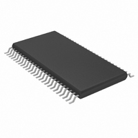
MAX9209EUM+D Maxim Integrated Products, MAX9209EUM+D Datasheet - Page 15

MAX9209EUM+D
Manufacturer Part Number
MAX9209EUM+D
Description
IC SERIALIZER PROG 48-TSSOP
Manufacturer
Maxim Integrated Products
Datasheet
1.MAX9209EUMD.pdf
(21 pages)
Specifications of MAX9209EUM+D
Function
Serializer
Data Rate
1.785Gbps
Input Type
LVTTL/LVCMOS
Output Type
LVDS
Number Of Inputs
21
Number Of Outputs
3
Voltage - Supply
3 V ~ 3.6 V
Operating Temperature
-40°C ~ 85°C
Mounting Type
Surface Mount
Package / Case
48-TSSOP
Lead Free Status / RoHS Status
Lead free / RoHS Compliant
R
Equation 1 is for two series capacitors (Figure 14). The
bit time (t
9. The DSV is 10. See equation 3 for four series capaci-
tors (Figure 15).
The capacitor for 2% maximum droop at 8MHz parallel
rate clock is:
Jitter due to droop is proportional to the droop and
transition time:
where:
t
t
D = droop (% of signal amplitude)
Jitter due to 2% droop and assumed 1ns transition time is:
The transition time in a real system depends on the fre-
quency response of the cable driven by the serializer.
The capacitor value decreases for a higher frequency
parallel clock and for higher levels of droop and jitter.
Use high-frequency, surface-mount ceramic capacitors.
Equation 1 altered for four series capacitors (Figure 15) is:
The MAX9209/MAX9213 have an integrated output ter-
mination resistor across each of the four LVDS outputs.
These resistors damp reflections from induced noise and
mismatches between the transmission line impedance
and termination resistor at the deserializer input. In DC-
balanced mode, the differential output resistance is part
of the RC time constant. In non-DC-balanced mode, the
output termination is increased to 410Ω (typ) to reduce
power. In power-down mode (PWRDWN = low) or when
the power supply is off, the output resistor is switched
out and the LVDS outputs are high impedance.
Driving PWRDWN low stops the PLL, switches out the
integrated output termination resistors, puts the LVDS
outputs in high impedance, and reduces supply current
J
T
O
C = -(2 x 13.9ns x 10) / (ln (1 - .02) x (100Ω + 78Ω))
= jitter (s)
= transition time (s) (0% to 100%)
C = -(4 x t
= output resistance (Ω)
C = -(2 x t
B
) is the period of the parallel clock divided by
B
x DSV) / (ln (1 - D) x (R
B
______________________________________________________________________________________
x DSV) / (ln (1 - D) x (R
t
J
t
C = 0.0773µF
J
= t
= 1ns x 0.02
t
J
T
PWRDWN and Power-Off
= 20ps
Integrated Termination
x D (Eq 2)
T
+ R
T
+ R
O
)) (Eq 3)
O
))
Programmable DC-Balanced
to 50µA or less. Driving PWRDWN high starts the PLL
lock to the input clock and switches in the output termi-
nation resistors. The LVDS outputs are not driven until
the PLL locks. The differential output resistance pulls
the outputs together and the LVDS outputs are high
impedance to ground. If the power supply is turned off,
the output resistors are switched out and the LVDS out-
puts are high impedance.
The PLL lock time is set by an internal counter. The maxi-
mum time to lock is 32,800 clock periods. Power and
clock should be stable to meet the lock-time specifica-
tion. When the PLL is locking, the LVDS outputs are not
active and have a differential output resistance of R
There are separate power domains for LVDS, PLL, and
digital circuits. Bypass each LVDS V
V
0.1µF and 0.001µF capacitors in parallel as close to the
device as possible, with the smallest value capacitor
closest to the supply pin.
The LVDS outputs are current sources. The voltage
swing is proportional to the load impedance. The out-
puts are rated for a differential load of 100Ω ±1%.
Interconnect for LVDS typically has a differential imped-
ance of 100Ω. Use cables and connectors that have
matched differential impedance to minimize impedance
discontinuities.
Twisted-pair and shielded twisted-pair cables offer
superior signal quality compared to ribbon cable and
tend to generate less EMI due to magnetic field cancel-
ing effects. Balanced cables pick up noise as common
mode, which is rejected by the LVDS receiver.
Keep the LVTTL/LVCMOS input and LVDS output sig-
nals separated to prevent crosstalk. A four-layer PCB
with separate layers for power, ground, LVDS outputs,
and digital signals is recommended.
CC
pin with high-frequency surface-mount ceramic
21-Bit Serializers
Power-Supply Bypassing
Cables and Connectors
PLL Lock Time
CC
LVDS Outputs
Board Layout
, PLL V
CC
O
, and
.
15


