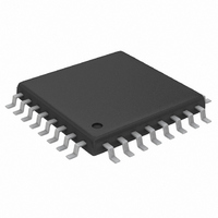
MAX3690ECJ Maxim Integrated Products, MAX3690ECJ Datasheet - Page 4

MAX3690ECJ
Manufacturer Part Number
MAX3690ECJ
Description
IC SERIALIZR 622MBPS TTL 32-TQFP
Manufacturer
Maxim Integrated Products
Datasheet
1.MAX3690ECJ.pdf
(8 pages)
Specifications of MAX3690ECJ
Function
Serializer
Data Rate
622Mbps
Input Type
TTL
Output Type
PECL
Number Of Inputs
8
Number Of Outputs
1
Voltage - Supply
3 V ~ 3.6 V
Operating Temperature
-40°C ~ 85°C
Mounting Type
Surface Mount
Package / Case
32-LQFP
Lead Free Status / RoHS Status
Contains lead / RoHS non-compliant
Available stocks
Company
Part Number
Manufacturer
Quantity
Price
Company:
Part Number:
MAX3690ECJ
Manufacturer:
MAXIM
Quantity:
2
Company:
Part Number:
MAX3690ECJ+
Manufacturer:
Maxim Integrated
Quantity:
10 000
Company:
Part Number:
MAX3690ECJ+T
Manufacturer:
Maxim Integrated
Quantity:
10 000
Company:
Part Number:
MAX3690ECJT
Manufacturer:
TI
Quantity:
2 934
The MAX3690 serializer comprises an 8-bit parallel
input register, an 8-bit shift register, control and timing
logic, a PECL output buffer, TTL input/output buffers,
and a frequency-synthesizing PLL (consisting of a
phase/frequency detector, loop filter/amplifier, voltage-
controlled oscillator, and programmable prescaler).
This device converts 8-bit-wide, 77Mbps parallel data
to 622Mbps serial data (Figure 1).
The PLL synthesizes an internal 622MHz reference
used to clock the output shift register. This clock is
generated by locking onto the external crystal refer-
ence clock signal (RCLK) operating at either
77.76MHz, 51.84MHz, or 38.88MHz. The incoming par-
+3.3V, 622Mbps, SDH/SONET 8:1 Serializer
with Clock Synthesis and TTL Inputs
4
_______________Detailed Description
______________________________________________________________Pin Description
18, 19, 24,
12, 13, 16,
21, 28, 29
9, 10, 17,
25, 26,
_______________________________________________________________________________________
31, 32
PIN
1–8
11
14
15
20
22
23
27
30
PD0–PD7
PCLKO
CKSET
NAME
PCLKI
RCLK
GND
SD+
FIL+
V
SD-
FIL-
CC
TTL Parallel-Data Inputs. Data is clocked in on the PCLKI signal’s positive transition.
Ground
TTL Parallel-Clock Output. Use positive transition of PCLKO to clock the overhead management
circuit.
+3.3V Supply Voltage
Inverting PECL Serial-Data Output
Noninverting PECL Serial-Data Output
Reference Clock Rate Programming Pin.
CKSET = open: Reference clock rate = 77.76MHz
CKSET = 20kΩ to GND: Reference clock rate = 51.84MHz
CKSET = GND: Reference clock rate = 38.88MHz
Filter Capacitor Input. Connect a 1µF capacitor between FIL- and V
Filter Capacitor Input. Connect a 1µF capacitor between FIL- and V
TTL Reference-Clock Input. Connect a crystal reference clock (77.76MHz, 51.84MHz or 38.88MHz) to
the RCLK input. The active edge is the positive transitioning edge.
TTL Parallel-Clock Input. Connect the incoming parallel-data-clock signal to the PCLKI input. The
active edge is the positive transitioning edge.
allel data is clocked into the MAX3690 on the rising
transition of the parallel-clock-input signal (PCLKI). The
control and timing logic ensure proper operation if the
parallel-input register is latched within a window of time
that is defined with respect to the parallel-clock-output
signal (PCLKO). PCLKO is the synthesized 622MHz
internal serial-clock signal divided by eight. Parallel-
clock output to parallel-clock-input delay (skew) must
be observed. Figure 2 shows the timing diagram.
The serial-data PECL outputs (SD+, SD-) require 50Ω
DC termination to (V
Output Termination section.
FUNCTION
CC
- 2V). See the Alternative PECL-
CC
CC
.
.
PECL Outputs


