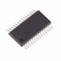
MAX9150EUI+ Maxim Integrated Products, MAX9150EUI+ Datasheet - Page 2

MAX9150EUI+
Manufacturer Part Number
MAX9150EUI+
Description
IC REPEATER LVDS 28-TSSOP
Manufacturer
Maxim Integrated Products
Type
Repeaterr
Datasheet
1.MAX9150EUI.pdf
(10 pages)
Specifications of MAX9150EUI+
Tx/rx Type
LVDS
Delay Time
2.2ns
Voltage - Supply
3 V ~ 3.6 V
Current - Supply
130mA
Mounting Type
Surface Mount
Package / Case
28-TSSOP
Lead Free Status / RoHS Status
Lead free / RoHS Compliant
Capacitance - Input
-
Lead Free Status / Rohs Status
Details
ABSOLUTE MAXIMUM RATINGS
V
RIN+, RIN- to GND ................................................-0.3V to +4.0V
PWRDN to GND..........................................-0.3V to (V
DO_+, DO_- to GND..............................................-0.3V to +4.0V
Short-Circuit Duration (DO_+, DO_-) .........................Continuous
Continuous Power Dissipation (T
Low-Jitter, 10-Port LVDS Repeater
DC ELECTRICAL CHARACTERISTICS
(V
unless otherwise noted. Typical values are at V
Stresses beyond those listed under “Absolute Maximum Ratings” may cause permanent damage to the device. These are stress ratings only, and functional
operation of the device at these or any other conditions beyond those indicated in the operational sections of the specifications is not implied. Exposure to
absolute maximum rating conditions for extended periods may affect device reliability.
2
CC
P W R D N
Input High Voltage
Input Low Voltage
Input Current
LVDS INPUT
Differential Input High Threshold
Differential Input Low Threshold
Single-Ended Input Current
Power-Off Single-Ended Input
Current
Differential Input Resistance
LVDS DRIVER
Differential Output Voltage
Change in VOD Between
Complementary Output States
Offset (Common-Mode) Voltage
Change in VOS Between
Complementary Output States
Output High Voltage
Output Low Voltage
Differential Output Resistance
(Note 2)
Differential High Output Voltage
in Fail-Safe
Output Short-Circuit Current
CC
28-Pin TSSOP (derate 12.8mW/°C above +70°C) .....1026mW
_______________________________________________________________________________________
to GND ...........................................................-0.3V to +4.0V
= +3.0V to +3.6V, R
PARAMETER
L
= 50Ω ±1%,
A
= +70°C)
SYMBOL
I
RO
IN(OFF)
RI
ΔV
ΔV
V
V
V
|
V
V
V
V
V
I
V
OD+
V
I
I
DIFF
SC
OD
OH
IN
IN
OS
TH
OL
TL
DIFF
IH
IL
OD
ID
OS
|
= 0.1V to 1.0V, V
CC
V
PWRDN = high or low; V
RIN- = open or RIN+ = open, V
PWRDN = high or low; V
RIN- = open or RIN+ = open, V
V
or RIN+ = open, V
V
Figure 1
Figure 1
Figure 1
Figure 1
Figure 1
Figure 1
V
R
100Ω termination
V
V
= +3.3V, T
IN
CC
CC
CC
IN+
ID
ID
CC
= V
= +100mV, V
= -100mV, V
= 0V; V
, R
= +3.6V or 0V, PWRDN = high or low
= +3.6V or 0V, PWRDN = high or low
+ 0.3V)
CC
IN-
undriven with short, open, or
and 0V
A
RIN+
CM
= +25°C.) (Note 1)
CONDITIONS
DO_-
=
= 2.4V, RIN- = open
DO_+
RIN-
|
V
Storage Temperature.........................................-65°C to +150°C
Maximum Junction Temperature .....................................+150°C
Operating Temperature Range...........................-40°C to +85°C
Lead Temperature (soldering, 10s) .................................+300°C
ID
= GND
= 2.4V
= GND
/ 2
RIN+
RIN+
|
to 2.4V -
= 2.4V,
= 0V,
RIN-
RIN-
= 2.4V
= 0V
|
V
ID
/ 2
|
, PWRDN = high, T
-100
0.90
MIN
250
150
250
2.0
-15
-18
0.7
-15
-6
-1
5
TYP
1.25
320
240
-7
7
A
= -40°C to +85°C,
1.375
MAX
100
+12
450
330
450
0.8
1.6
15
+1
+1
25
25
UNITS
mV
mV
mV
mV
mV
mV
mA
kΩ
µA
µA
µA
Ω
V
V
V
V
V


